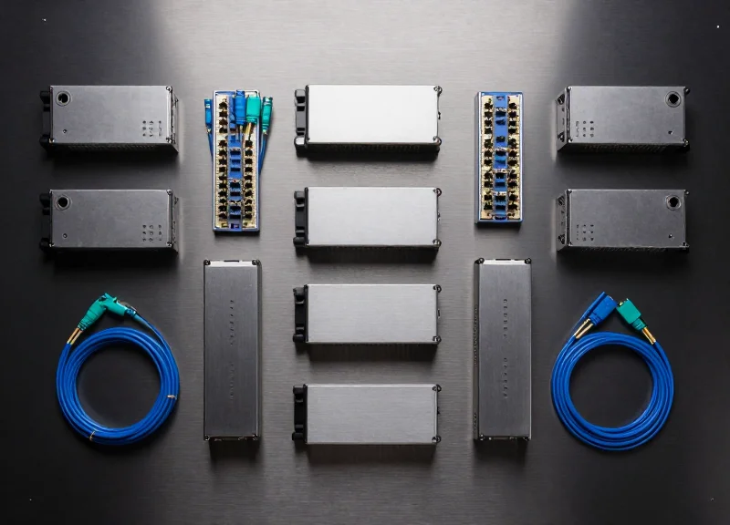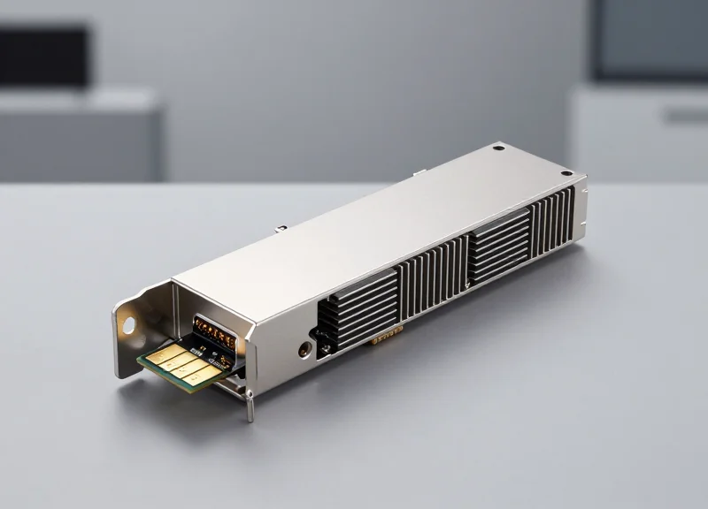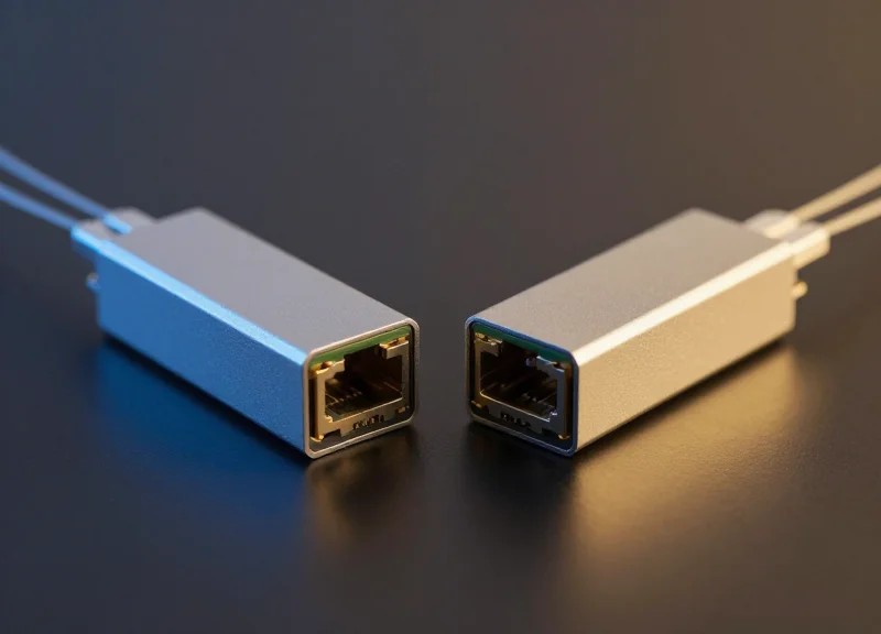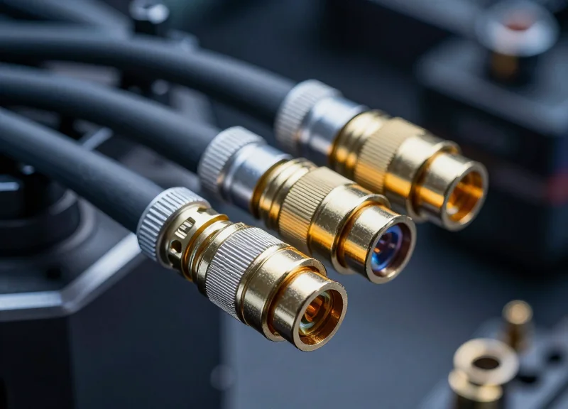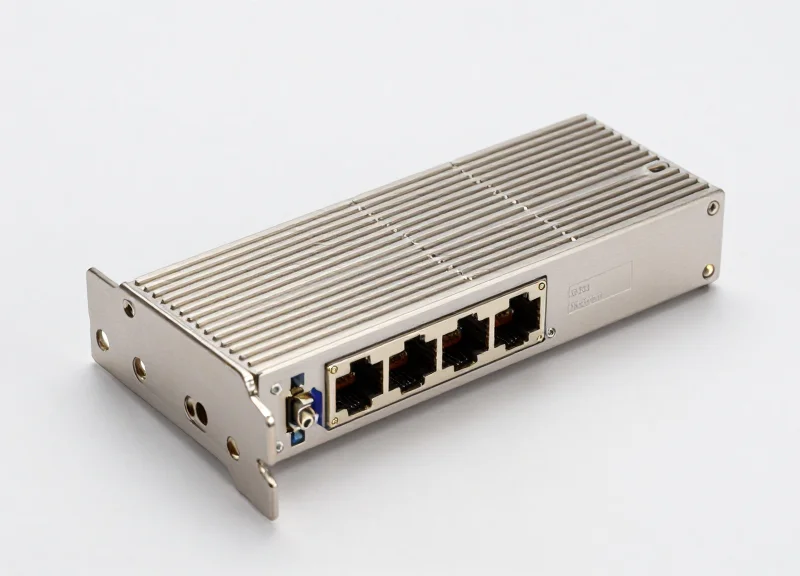
As global data traffic explodes, the supply chain for optical components has become the backbone of modern digital infrastructure. This article provides a comprehensive technical breakdown of how optics are designed, manufactured, and distributed to meet the demands of AI and 5G networks.
The Anatomy of the Optical Supply Chain

The Hierarchical Structure of Optical Hardware Production
The global supply chain for optics is a highly specialized vertical hierarchy that begins with the synthesis of ultra-pure materials and terminates with the deployment of high-capacity transport networks. Unlike commodity electronics, the optical supply chain is defined by 'photonic-grade' tolerances, where the slightest impurity in a glass preform or a nanometer-scale misalignment in a transceiver assembly can render an entire production batch non-functional. This anatomy is divided into four distinct tiers, each adding layers of complexity through materials science, semiconductor fabrication, and systems engineering.
Tier 4 and 3: The Foundational Layer of Materials and Components
At the base of the chain are the providers of raw chemical substrates and optical glass. These companies produce the high-purity silica used for fiber optic cabling and the exotic semiconductors required for active components. Tier 3 players take these materials to create discrete components, such as laser diodes, photodetectors, and passive filters.
| Substrate Material | Primary Application | Key Technical Advantage |
|---|---|---|
| Silicon (Si) | Silicon Photonics / PICs | CMOS compatibility for high-volume scaling |
| Indium Phosphide (InP) | High-performance Lasers | Efficient light emission at C-band wavelengths |
| Lithium Niobate (LiNbO3) | High-speed Modulators | Excellent electro-optic coefficient for 800G+ rates |
| Synthetic Quartz | Optical Fiber Preforms | Ultra-low attenuation for long-haul transmission |
Tier 2 and 1: Integration and Systems Engineering
Tier 2 consists of module integrators who package discrete components into standardized form factors, such as QSFP-DD or OSFP transceivers. This stage involves complex optical-electrical-optical (OEO) conversions and sophisticated Digital Signal Processing (DSP) integration. Finally, Tier 1 System OEMs (Original Equipment Manufacturers) incorporate these modules into macro-scale hardware like ROADMs and DWDM platforms, which are sold to the end-users: Tier 0 network operators and hyperscale data centers.
- What is the primary bottleneck in the optical supply chain?
The production of high-performance DSPs and specialized semiconductor wafers (like InP) remains the tightest bottleneck due to the limited number of specialized fabrication plants (fabs) capable of meeting photonic standards. - How does 'vertical integration' affect this anatomy?
Some Tier 1 providers are vertically integrated, meaning they design their own Tier 3 components and Tier 2 modules to ensure better performance optimization and supply chain resilience. - Who are the 'Tier 0' players in this model?
Tier 0 refers to the end-users, primarily Global Tier 1 ISPs, Content Delivery Networks (CDNs), and Hyperscale Cloud Providers who operate the finished infrastructure.
Raw Material Sourcing: From Silicon to Indium Phosphide
The raw material stage of the optical supply chain is defined by the transition from bulk chemical elements to high-purity crystalline substrates. While silicon is the dominant material for electronic integrated circuits, the physics of light generation requires III-V compound semiconductors like Indium Phosphide (InP) and Gallium Arsenide (GaAs). These materials are essential because they possess a direct bandgap, allowing for the efficient radiative recombination of electrons and holes to produce photons—a feat that silicon, with its indirect bandgap, cannot naturally achieve.
Substrate Characteristics and Material Selection
Choosing a substrate involves balancing optical performance, thermal conductivity, and manufacturing scale. Silicon Photonics (SiPh) has emerged as a disruptive force by leveraging the massive scale of the CMOS industry, though it still relies on external or heterogeneously integrated III-V materials for the light source itself.
| Material | Bandgap Type | Primary Optical Use | Manufacturing Maturity |
|---|---|---|---|
| Silicon (Si) | Indirect | Passive Waveguides, Modulators | Very High (CMOS) |
| Indium Phosphide (InP) | Direct | Active Lasers, Amplifiers | Moderate |
| Gallium Arsenide (GaAs) | Direct | VCSELs, Short-reach Transceivers | High |
| Lithium Niobate (LiNbO3) | N/A (Insulator) | High-speed Modulators | Moderate |
Indium Phosphide (InP): The Critical Path for Coherent Optics
For long-haul and high-capacity data center interconnects, Indium Phosphide is the gold standard. Its lattice constant allows for the growth of quaternary alloys like InGaAsP, which can be tuned to emit light at 1310 nm (O-band) and 1550 nm (C-band). These wavelengths coincide with the minimum dispersion and attenuation windows of silica optical fiber. Sourcing InP involves complex chemical vapor deposition (CVD) processes and the procurement of high-purity Indium, which is often a byproduct of zinc mining, making the supply chain sensitive to industrial metal market fluctuations.
Supply Chain Fragility and Geopolitics
The concentration of raw material processing for elements like Gallium and Indium poses a significant risk to the optical supply chain. A majority of the world's high-purity gallium is refined in specific geographic regions, leading to potential bottlenecks if trade restrictions are implemented. Furthermore, the synthesis of high-quality crystalline ingots requires specialized equipment (such as Molecular Beam Epitaxy or Metal-Organic Chemical Vapor Deposition reactors) that is produced by only a handful of companies globally.
Common Questions on Optical Raw Materials
- Why can't we use silicon for all optical components?
Silicon has an indirect bandgap, meaning it is extremely inefficient at emitting light. While it is excellent for routing light (waveguides) and processing electrical signals, it cannot serve as the primary material for the laser source. - What makes Indium Phosphide so expensive compared to Silicon?
InP wafers are smaller (typically 2 to 6 inches) compared to Silicon wafers (up to 12 inches), and the growth process is more difficult, resulting in lower yields and higher costs per square inch. - Are there alternatives to Indium and Gallium?
Research is ongoing into Silicon-Germanium (SiGe) and quantum dot lasers on silicon, but currently, III-V compounds remain the only commercially viable solution for high-performance laser diodes.
Wafer Fabrication and Silicon Photonics

Wafer Fabrication and Silicon Photonics
Silicon photonics (SiPh) represents the convergence of electronics and optics, utilizing existing high-volume semiconductor manufacturing processes to create Photonic Integrated Circuits (PICs). By repurposing the mature Complementary Metal-Oxide-Semiconductor (CMOS) infrastructure, the industry can fabricate complex optical systems—including modulators, waveguides, and photodetectors—on standard 300mm silicon-on-insulator (SOI) wafers. This transition from discrete assembly to monolithic or heterogeneous wafer-level integration is the primary driver behind the miniaturization and cost reduction of modern optical transceivers.
The Shift to Silicon-on-Insulator (SOI) Substrates
Unlike standard logic chips that use bulk silicon, silicon photonics predominantly uses SOI wafers. These wafers feature a thin layer of crystalline silicon separated from the substrate by a buried oxide (BOX) layer. The refractive index contrast between the silicon and the oxide creates a highly efficient waveguide, allowing light to be confined and routed with minimal loss. This structural advantage enables the dense integration of optical functions alongside electrical circuits, bridging the gap between data processing and high-speed data transmission.
| Feature | Traditional Discrete Optics | Silicon Photonics (SiPh) |
|---|---|---|
| Manufacturing | Manual/Semi-automated assembly | Automated wafer-scale CMOS fab |
| Integration Density | Low; discrete components | High; thousands of functions per chip |
| Power Consumption | High (OEO conversions) | Low (Integrated modulation) |
| Scalability | Limited by labor and yields | High volume via semiconductor foundries |
Heterogeneous Integration: Solving the Light Source Dilemma
One of the greatest technical hurdles in wafer fabrication for optics is that silicon is an indirect bandgap material, making it an inefficient light emitter. To solve this, the supply chain utilizes heterogeneous integration, where III-V materials (like Indium Phosphide) are bonded to the silicon wafer at the die or wafer level. Techniques such as flip-chip bonding or molecular wafer bonding allow foundries to incorporate the laser source directly into the silicon photonic circuit, creating a complete 'system-on-a-chip' that eliminates the need for external fiber coupling between the laser and the modulator.
- Why is CMOS compatibility important for optics?
CMOS compatibility allows optical components to be manufactured using the same multi-billion dollar fabrication plants used for CPUs and memory, ensuring high yields, extreme precision, and rapid scalability. - What is the role of foundries like TSMC and GlobalFoundries in this chain?
These foundries provide specialized 'Silicon Photonics' process design kits (PDKs) that allow fabless designers to create optical circuits that are guaranteed to work within the foundry's specific manufacturing tolerances. - How does silicon photonics reduce power consumption?
By placing the optical interface closer to the electrical switch (co-packaged optics), the energy required to drive high-speed signals across long copper traces on a PCB is eliminated.
As the industry moves toward 800G and 1.6T transmission speeds, the role of the foundry becomes even more critical. The precision of lithography machines (EUV/DUV) directly impacts the phase error and insertion loss of waveguides. Consequently, the global supply chain is seeing a consolidation of power among a few tier-1 foundries capable of maintaining the sub-nanometer tolerances required for high-performance silicon photonics.
Packaging and Assembly: The Role of OSATs
Packaging and Assembly: The Role of OSATs
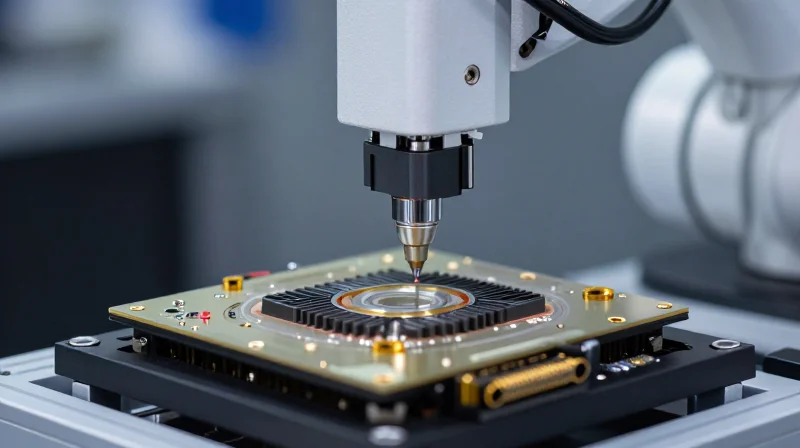
Outsourced Semiconductor Assembly and Test (OSAT) providers are the bridge between raw wafer fabrication and the finished optical module, responsible for the complex task of integrating Photonic Integrated Circuits (PICs) with electronic components. In the optical supply chain, OSATs perform 'back-end' processes that include die-attach, wire bonding, and the critical attachment of fiber-optic pigtails. Unlike standard electronics, optical packaging requires sub-micron alignment tolerances and specialized materials to maintain signal integrity over the device's lifespan.
The Challenge of Sub-Micron Alignment
The most significant differentiator for an optical OSAT is the requirement for active alignment. While traditional chip placement allows for several microns of shift, optical fibers must be aligned to laser diodes or waveguides with tolerances often tighter than 0.5 microns. OSATs utilize automated vision systems and 'active' feedback loops, where the laser is powered on during the bonding process to find the peak optical power coupling point before the adhesive or solder is UV-cured or cooled.
Thermal Management and Material Science
High-speed optical transceivers generate significant heat concentrated in small areas, particularly within the laser driver and the laser diode itself. OSATs must implement sophisticated thermal management strategies, such as the use of High-Thermal Conductivity (HTC) substrates like Aluminum Nitride (AlN) or Silicon Carbide (SiC). Additionally, Thermoelectric Coolers (TECs) are often integrated directly into the package to stabilize the laser's operating temperature, preventing wavelength drift and ensuring long-term reliability in data center environments.
| Packaging Technology | Alignment Precision | Thermal Management | Typical Application |
|---|---|---|---|
| Chip-on-Board (COB) | Low to Medium | Passive Heat Sinks | Short-reach VCSELs |
| Gold Box / TOSA | High (Active) | Integrated TEC | Long-haul Telecom |
| Co-Packaged Optics (CPO) | Ultra-High | Advanced Liquid/Cold Plate | Next-gen AI Switches |
Technical FAQ: Optical OSAT Operations
- What is the difference between active and passive alignment?
Passive alignment relies on physical markers and high-precision pick-and-place machines to align components, whereas active alignment involves powering the device and monitoring real-time light throughput to optimize position before final bonding. - Why is CTE mismatch a major concern in optical packaging?
The Coefficient of Thermal Expansion (CTE) mismatch between the silicon chip, the glass fiber, and the metallic package can cause physical shifting during temperature cycles, leading to 'optical misalignment' and total signal loss. - How do OSATs ensure the hermeticity of optical packages?
OSATs use laser welding or specialized glass-to-metal seals to create hermetic environments that protect sensitive III-V materials from moisture and oxidation, though many modern designs are moving toward 'non-hermetic' packaging for cost reduction.
Standardization and Multi-Source Agreements (MSAs)
Standardization and Multi-Source Agreements (MSAs)
In the global optics supply chain, Multi-Source Agreements (MSAs) serve as the technical bedrock that allows components from different manufacturers to function interchangeably within a single network ecosystem. By defining precise mechanical dimensions, electrical interfaces, and management protocols, MSAs ensure that a transceiver produced in a Shenzhen facility is fully compatible with a switch manufactured in the United States and deployed in a European data center. This interoperability is what prevents the market from fragmenting into proprietary silos, thereby driving down costs through healthy competition and economies of scale.
The Distinction Between Standards and MSAs
While often used interchangeably, there is a technical distinction between formal standards and MSAs. Formal standards bodies, such as the IEEE (Institute of Electrical and Electronics Engineers), focus on the 'logical' side, such as the 800G Ethernet protocol or signal modulation techniques like PAM4. In contrast, MSAs are industry-led consortia that define the 'physical' and 'management' implementation. For example, the QSFP-DD MSA defines the physical plug, while the OIF (Optical Internetworking Forum) defines the Common Management Interface Specification (CMIS) that allows the software to communicate with the hardware regardless of the vendor.
| MSA Form Factor | Target Throughput | Thermal Management | Supply Chain Role |
|---|---|---|---|
| QSFP-DD | 400G / 800G | External Heat Sink Required | Mainstream Data Center Standard |
| OSFP | 800G / 1.6T | Integrated Heat Sink | High-Power AI/ML Clusters |
| SFP-DD | 100G | Passive/Active Cooling | Edge and Enterprise Access |
| QSFP28 | 100G | Standard Passive | Legacy Core and Metro Links |
Interoperability as a Risk Mitigation Strategy
For global supply chain managers, standardization is a primary tool for risk mitigation. Without MSAs, an operator would be 'vendor-locked' to a single manufacturer's proprietary design. If that manufacturer faces a factory shutdown or a raw material shortage, the operator's entire network expansion could grind to a halt. By adhering to MSA specifications, procurement teams can qualify multiple sources (dual-sourcing or multi-sourcing), ensuring that if one supplier fails, another can provide a technically identical component to fill the gap.
- How do MSAs affect lead times?
By standardizing parts, manufacturers can build 'generic' hardware platforms in advance, only finalizing the firmware or laser wavelengths once an order is placed, significantly reducing fulfillment times. - What is the role of CMIS in the supply chain?
The Common Management Interface Specification (CMIS) ensures that different modules provide the same diagnostic data to host systems, simplifying software integration for network operators across diverse hardware. - Why do new MSAs emerge frequently?
As data rates increase from 400G to 1.6T, previous form factors often cannot handle the heat dissipation or signal integrity requirements, necessitating new agreements for larger or more thermally efficient designs.
Testing and Quality Assurance Protocols
Testing and Quality Assurance Protocols
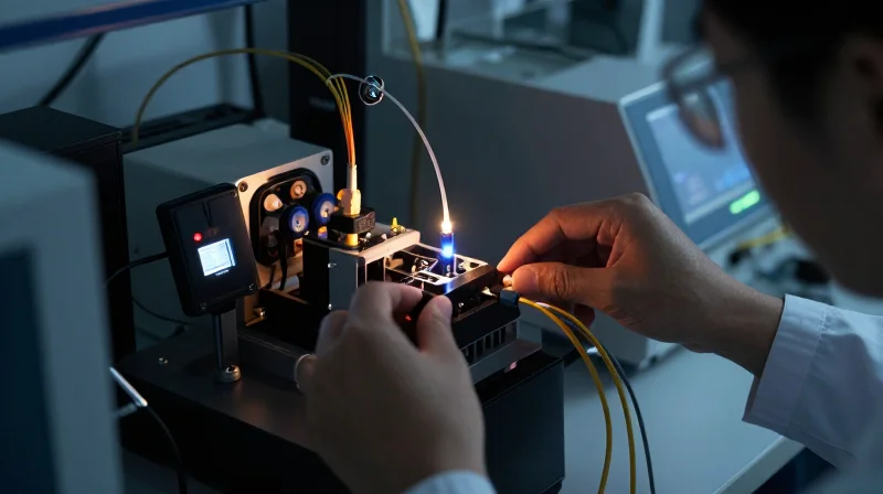
Testing and Quality Assurance (QA) protocols in the global optics supply chain serve as the ultimate validation layer, employing advanced methodologies like Bit Error Rate (BER) analysis, Eye Diagram testing, and Environmental Stress Screening (ESS) to ensure that high-speed transceivers and passive components meet the stringent reliability demands of modern hyperscale data centers and telecommunications networks.
Core Performance Metrics for Optical Interconnects
Quantifying the health of an optical link requires precise measurement of signal integrity. In high-speed optics (400G and beyond), the focus shifts from simple power levels to complex modulation analysis, particularly for PAM4-encoded signals where noise margins are significantly tighter.
| Metric | Technical Definition | Industry Benchmark |
|---|---|---|
| Bit Error Rate (BER) | The ratio of erroneous bits to the total number of transmitted bits. | < 1E-12 (Post-FEC) |
| TDECQ | Transmitter and Dispersion Eye Closure Quaternary; measures PAM4 signal quality. | < 3.4 dB (IEEE 802.3bs) |
| Extinction Ratio (ER) | The ratio of the power level for a logic '1' to the power level for a logic '0'. | > 3.5 dB (for most SMF applications) |
| Optical Return Loss (ORL) | A measure of the light reflected back toward the source. | > 20-30 dB depending on connector type |
Environmental Stress Screening (ESS) and Reliability
Because optical modules are deployed in environments ranging from climate-controlled enterprise server rooms to unconditioned edge computing cabinets, the supply chain must include rigorous environmental testing. This includes 'Burn-in' phases where modules are operated at elevated temperatures (typically 70°C to 85°C) for 24 to 72 hours to precipitate infant mortality failures. Further testing involves thermal cycling, where components are rapidly transitioned between extreme temperatures to test the mechanical integrity of epoxy bonds and laser alignments.
Automated Test Equipment (ATE) and Scaling
To handle the volume requirements of the global market, manufacturers utilize Automated Test Equipment (ATE). These systems integrate optical spectrum analyzers, bit error rate testers (BERTs), and digital communication analyzers into a single workflow. ATE reduces human error and provides a 'birth certificate' for every module—a serialized data log that tracks performance metrics from the wafer level to the final assembly, facilitating traceability in the event of field failures.
Frequently Asked Questions
- Why is Forward Error Correction (FEC) important in QA?
As data rates increase, signal-to-noise ratios decrease. FEC allows the system to correct small numbers of bit errors, enabling modules to pass quality gates even if their raw (pre-FEC) BER is relatively high, provided the post-FEC result is error-free. - What is the difference between design validation and production testing?
Design validation (DVT) is an exhaustive process on a small sample size to ensure the design meets all specs, while production testing is a streamlined set of tests performed on every unit to ensure manufacturing consistency. - How does moisture affect optical supply chain QA?
High humidity can lead to the 'fogging' of internal lenses or the degradation of delicate laser facets. QA protocols often include Damp Heat testing (85% humidity at 85°C) to ensure hermetic or non-hermetic packaging holds up over time.
Logistics and Just-in-Time Delivery for Data Centers

Logistics and Just-in-Time Delivery for Data Centers
The global supply chain for high-speed optics has transitioned from bulk warehousing to a Just-in-Time (JIT) delivery model, driven by the high unit cost of 400G/800G transceivers and the rapid pace of hardware iteration. This approach synchronizes manufacturing output with data center site readiness, ensuring that thousands of optical modules arrive at the facility only when the corresponding network switches are ready for population, thereby reducing the financial burden of stagnant inventory and the risk of deploying outdated firmware.
Strategic Lead Time Management for 800G Deployments
Managing lead times for 800G optics is complex due to the reliance on cutting-edge Digital Signal Processors (DSPs) and specialized laser components. To mitigate volatility, hyperscalers employ rolling 12-month forecasts and 'component pre-staging,' where critical long-lead sub-components are purchased in advance by the manufacturer while the final assembly is deferred until the JIT window opens. This hybrid strategy provides a buffer against supply shocks without committing to finished goods too early.
| Feature | Traditional Warehousing | Just-in-Time (JIT) Delivery |
|---|---|---|
| Inventory Holding Costs | High - requires significant upfront capital | Low - optimized for cash flow management |
| Firmware Consistency | Risk of 'stale' firmware in long-term storage | High - latest versions applied at time of shipping |
| Responsibility for Stock | Buyer (Data Center Operator) | Supplier or 3PL (Vendor Managed Inventory) |
| Transport Frequency | Low frequency, high volume | High frequency, precision volume |
Regional Hubbing and Risk Mitigation
Regional hubbing serves as the backbone of JIT logistics. By establishing localized distribution centers in proximity to major data center clusters, vendors can provide same-day or next-day delivery services. These hubs often perform 'last-mile' value-added services, such as customer-specific labeling, final performance verification, and environmental screening, which shifts the final quality gate closer to the point of use.
- How do lead times differ between 400G and 800G?
400G optics have a more mature supply chain with lead times typically under 12 weeks, whereas 800G optics can extend to 20 or more weeks depending on DSP allocation and assembly yields. - What is the role of 3PLs in optical logistics?
Third-party logistics providers (3PLs) manage customs, bonded warehousing, and localized transport, often integrating their ERP systems with the hyperscaler's procurement platform for real-time visibility. - How is transit risk managed for sensitive optics?
High-speed modules are transported in specialized ESD-safe packaging and often utilize air freight for the main leg of transit to minimize the vibration and temperature exposure common in sea or rail freight.
Geopolitical Factors and Supply Chain Resilience
Geopolitical Factors and Supply Chain Resilience
In the context of the global supply chain for optics, geopolitical factors represent a critical risk layer that dictates the movement of high-tech components such as Indium Phosphide (InP) wafers, Silicon Photonics (SiPh) dies, and advanced TOSA/ROSA assemblies. As optical networks become the backbone of national security and economic competitiveness, trade policies, export controls, and regional manufacturing shifts are no longer just economic considerations—they are technical constraints that determine the availability and cost of 400G and 800G transceivers.
The Impact of Trade Policies and Export Controls
Export controls on critical semiconductor technologies, particularly high-performance Digital Signal Processors (DSPs) and advanced lithography tools, directly impact the production capacity of optical modules. Tariffs imposed on high-value components often force manufacturers to relocate final assembly and test (FAT) operations to neutral territories to maintain price competitiveness in the global market. These policy shifts can lead to sudden lead-time extensions if a primary manufacturing hub is restricted from accessing proprietary US or European IP.
| Region | Manufacturing Strength | Key Risk Factors |
|---|---|---|
| East Asia (China) | Massive scale, established ecosystem for sub-components. | Tariffs, export restrictions on advanced chipsets. |
| Southeast Asia (Vietnam/Thailand) | Growing assembly and testing (FAT) capabilities. | Developing ecosystem; reliance on imported raw materials. |
| North America / Europe | High-end R&D, SiPh design, and wafer fabrication. | Higher labor costs; limited capacity for high-volume assembly. |
| Central/South America (Mexico) | Proximity to US hyperscalers; low logistics latency. | Early stage for complex optical component fabrication. |
Strategic Diversification and Friend-Shoring
To mitigate the risk of single-point failures, optical transceiver manufacturers are increasingly adopting a 'China Plus One' strategy. This involves maintaining large-scale production facilities in established hubs while simultaneously spinning up redundant lines in regions like Malaysia or Vietnam. This diversification ensures that even if a specific trade corridor is blocked or heavily taxed, the supply of critical optics for hyperscale data centers remains uninterrupted. This shift also encourages the development of localized supply chains where raw materials and sub-assemblies are sourced within the same geopolitical bloc.
- How do export controls affect 800G optics?
Export controls often limit the transfer of the most advanced DSP technology and laser fabrication equipment, which can slow down the deployment of 800G and 1.6T modules in certain jurisdictions. - What is 'Friend-Shoring' in the optics industry?
It is the practice of focusing supply chain operations in countries that share similar political and economic values, reducing the likelihood of sudden trade disruptions or IP theft. - Are raw materials like Gallium and Germanium at risk?
Yes, as these are essential for III-V semiconductor manufacturing, export restrictions on these raw materials by major producers can create bottlenecks at the very start of the optical component lifecycle.
Ultimately, supply chain resilience in optics is achieved through a combination of technical standardization and geographic agility. By utilizing Multi-Source Agreements (MSAs) and diversified manufacturing, the industry ensures that the failure of one regional hub does not lead to a global blackout of optical connectivity.
Future Innovations: Co-Packaged Optics (CPO) and 1.6T

The Infrastructure Shift to 1.6T and Co-Packaged Optics
As data center requirements exceed the physical limits of traditional copper and even existing pluggable optical interfaces, the supply chain is reconfiguring to support 1.6T transceivers and the eventual integration of optics directly onto the switch silicon via CPO. This transition is not merely a speed upgrade but a fundamental redesign of how light is processed and managed within the networking stack. The move to 1.6T utilizes 224G SerDes lanes, which pushes the boundaries of signal integrity and requires advanced Digital Signal Processors (DSPs) and high-bandwidth lasers that currently face limited yields in the global market.
Technical Comparison: Pluggable 1.6T vs. Co-Packaged Optics
| Feature | 1.6T Pluggable | Co-Packaged Optics (CPO) | |||
|---|---|---|---|---|---|
| Form Factor | OSFP-XD / QSFP-DD1600 | On-board / Substrate Integrated | |||
| Power Consumption | Highest per bit (~25-30W) | 30-40% reduction vs. pluggable | |||
| Serviceability | High (Field replaceable) | Low (Integrated with ASIC) | Latency | Standard DSP latency | Lower (Shorter electrical traces) |
| Supply Chain Maturity | Established Ecosystem | Emerging (Requires Foundry/OSAT collab) |
The Supply Chain Evolution for CPO
The implementation of CPO disrupts the traditional vendor-customer relationship by moving the optical interface into the switch package. This shift necessitates a new collaborative model between switch ASIC vendors, silicon photonics foundries, and Outsourced Semiconductor Assembly and Test (OSAT) providers. For the first time, optical components must survive the same high-temperature reflow processes as advanced logic chips, demanding a total overhaul of materials science and testing protocols within the optics supply chain. Furthermore, External Laser Sources (ELS) are becoming a critical sub-segment, as they decouple the heat-sensitive laser from the switch ASIC to improve reliability.
- What is the primary driver for 1.6T adoption?
The exponential growth of AI/ML workloads requires higher radix switches and massive interconnect bandwidth that 800G cannot satisfy efficiently. - How does CPO impact optical testing?
CPO requires wafer-level optical testing and known-good-die (KGD) strategies, moving quality assurance earlier in the semiconductor manufacturing flow. - Will 1.6T pluggables be the final generation?
Industry consensus suggests 1.6T or 3.2T may be the final limit for pluggables before thermal density forces a widespread shift to CPO or Near-Packaged Optics (NPO). - Who are the key players in the 1.6T supply chain?
The ecosystem includes DSP giants like Marvell and Broadcom, laser suppliers like Lumentum, and transceiver manufacturers like Innolight and Coherent.
Looking forward, the global supply chain must solve the yield challenges of 200G-per-lane optics and the thermal management issues of integrating lasers into the cooling loop of the switch. Success in the 1.6T era will depend on the industry's ability to standardize the CPO ecosystem, ensuring interoperability between disparate components produced across the global semiconductor landscape.
Navigating the complexities of the global optics supply chain is critical for maintaining network uptime and scalability. To optimize your optical procurement strategy and ensure hardware compatibility, contact our technical consulting team today for a comprehensive network audit.