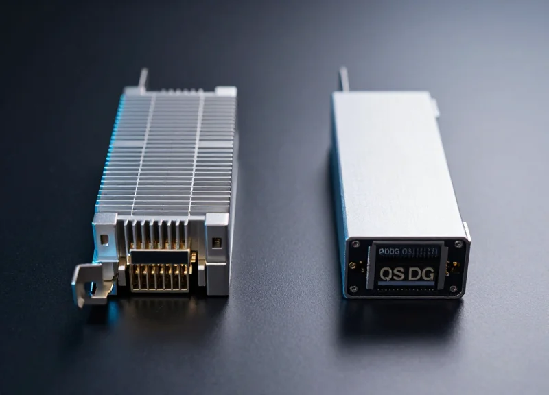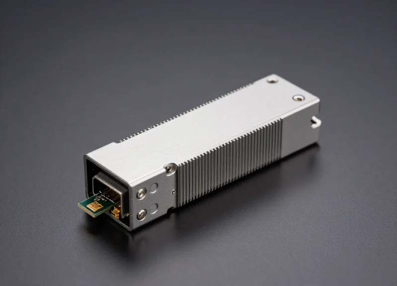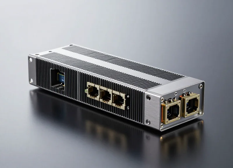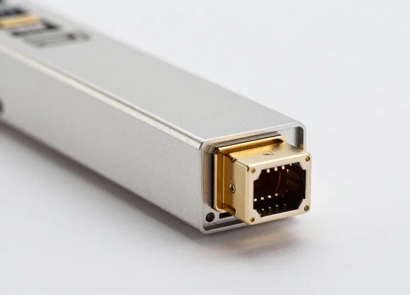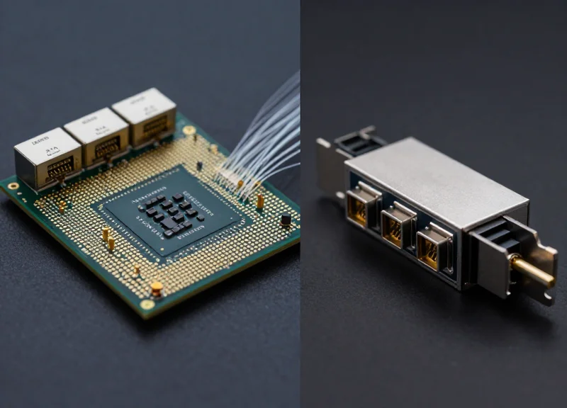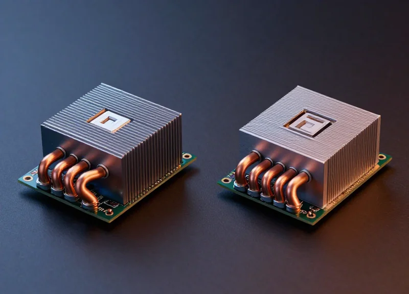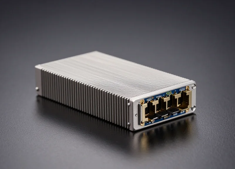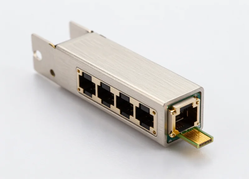
The explosive growth of AI/ML workloads and high-performance computing is pushing traditional networking hardware to its physical limits. As we transition beyond 800G toward 1.6T and 3.2T speeds, the energy consumed by moving data between switch ASICs and pluggable transceivers is becoming unsustainable. Co-Packaged Optics (CPO) represents a paradigm shift, moving the optical engine inside the package to drastically reduce power consumption and increase bandwidth density.
Defining Co-Packaged Optics (CPO)
Defining Co-Packaged Optics (CPO)
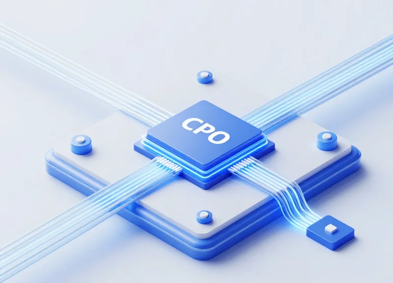
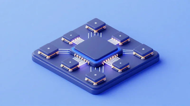
Co-Packaged Optics (CPO) is a sophisticated packaging technology that integrates optical transceivers and silicon photonics directly with high-bandwidth compute or switching application-specific integrated circuits (ASICs) on a single common substrate. By eliminating the physical distance between the processing silicon and the optical interface, CPO addresses the mounting power and density challenges inherent in the next generation of 51.2T and 102.4T networking switches.
The Architecture of Proximity
Traditionally, optical connectivity has relied on pluggable modules like QSFP-DD or OSFP inserted into the front panel of a switch. However, as data rates increase, the electrical traces required to carry signals from the ASIC across the PCB to these front-panel ports suffer from significant signal degradation and high power consumption. CPO solves this by bringing the 'optical engine' into the heart of the device, effectively shortening the electrical link to a few millimeters and reducing the need for high-power SerDes.
| Feature | Pluggable Optics | Co-Packaged Optics (CPO) |
|---|---|---|
| Interface Location | Front Panel / Faceplate | Internal Substrate / ASIC Package |
| Electrical Trace Length | Long (up to 10-15 inches) | Short (Millimeters) |
| Power Efficiency | Lower (due to SerDes overhead) | Optimized (lower power per bit) |
| Serviceability | Field replaceable per module | Substrate-level integration / Remote Laser |
| Bandwidth Density | Limited by faceplate area | High (Silicon-level scaling) |
Core Mechanisms and Architectural Requirements
- Why is CPO necessary for 800G and 1.6T systems?
As speeds exceed 800G per port, the electrical loss in traditional PCB materials becomes prohibitive, making CPO the only viable path to maintain signal integrity while keeping thermal loads manageable. - What is the role of the External Laser Source (ELS)?
To manage thermal dissipation and laser reliability, the laser source is often decoupled from the CPO package in a 'Remote Laser' configuration, allowing the light source to be replaced without disturbing the ASIC. - How does it differ from Near-Packaged Optics (NPO)?
While CPO places the optics on the ASIC substrate itself, NPO places the optical engines on the motherboard adjacent to the ASIC, serving as an intermediate step between pluggables and full CPO integration.
The Death of the Front-Panel: Why Pluggables Are Reaching a Wall
The Death of the Front-Panel: Why Pluggables Are Reaching a Wall
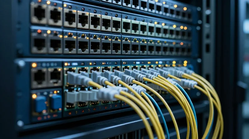
Traditional pluggable transceivers have sustained data center growth for decades, but the industry is now confronting a fundamental 'Power Wall' where the energy consumed simply to transport electrical signals across a PCB is becoming unsustainable. At the 51.2T switch generation, and certainly by 102.4T, the electrical SerDes (Serializer/Deserializer) required to drive signals from the switch ASIC to the front-panel modules consume nearly 30% of the total system power, leaving little headroom for the compute or switching silicon itself.
The Signal Integrity Crisis at 224Gbps
As per-lane speeds transition from 112Gbps to 224Gbps, the insertion loss over standard PCB materials like FR-4 or even advanced Megtron-7 becomes prohibitive. To maintain signal integrity over the 6 to 10 inches between the ASIC and the front panel, engineers are forced to use retimers and more robust PCB materials, both of which increase costs and thermal output. Co-packaged optics (CPO) solve this by reducing the electrical trace length to millimeters, effectively bypassing the physics-based limitations of copper interconnects.
| Parameter | Pluggable Optics (1.6T) | Co-Packaged Optics (CPO) |
|---|---|---|
| Trace Length (ASIC to Optical) | 150mm - 250mm | < 10mm |
| Power Efficiency | ~25-30 pJ/bit | < 10 pJ/bit |
| Faceplate Density | Limited by physical module size | Significantly higher (MPO/SN connectors) |
| Thermal Management | Localized heat on faceplate | Heat spread across ASIC substrate |
The Thermal Density Challenge
Faceplate real estate is a finite resource. A standard 1RU (Rack Unit) switch chassis can only accommodate a specific number of QSFP-DD or OSFP modules. As these modules reach 1.6T, they generate between 25W and 40W of heat each. Cooling 32 of these modules in a single chassis requires massive airflow and high-RPM fans, leading to a 'Thermal Wall' where the energy spent on cooling the optics exceeds the energy used to transmit data.
- Why can't we just improve SerDes efficiency?
While SerDes technology improves with each CMOS node, the physics of dielectric loss in copper traces does not change. The energy required to compensate for that loss via equalization and FEC grows exponentially with frequency. - Is 1.6T the definitive end for pluggables?
Many industry experts believe 1.6T will be the final density 'peak' for pluggables in high-end switches. Beyond this, the complexity and power overhead of electrical signaling will force a transition to CPO or Near-Packaged Optics (NPO). - Does CPO eliminate the need for front-panel connectors?
No, but it changes their nature. Instead of bulky electrical-to-optical modules, the front panel will feature high-density passive fiber connectors, significantly increasing the total bandwidth per rack unit.
Technical Architecture: Integrating Silicon Photonics and ASICs
Technical Architecture: Integrating Silicon Photonics and ASICs
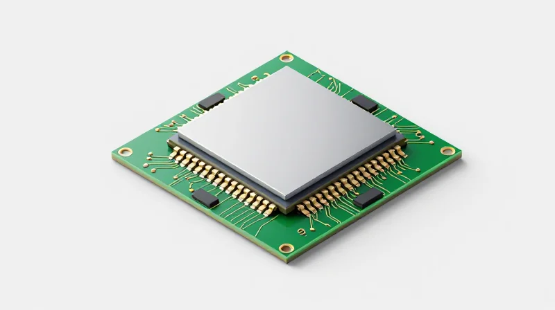
The core architectural innovation of Co-Packaged Optics (CPO) is the elimination of the long, lossy electrical traces between the switch ASIC and the optical transceiver. By moving the optical engine off the front panel and onto a common substrate with the compute silicon, the industry is shifting from a Pluggable-on-Board model to a Multi-Chip Module (MCM) approach. This integration allows for significantly reduced SerDes (Serializer/Deserializer) power consumption, as the electrical signals only need to travel millimeters across an organic or silicon interposer rather than centimeters across a PCB to a faceplate.
The Multi-Chip Module (MCM) Integration
In a CPO architecture, the host ASIC—typically a high-radix switch chip—is surrounded by multiple optical 'tiles' or engines. These engines are essentially Silicon Photonics (SiPh) dies that convert high-speed electrical signals into optical signals using integrated modulators and photodetectors. The physical integration is achieved through advanced packaging techniques like 2.5D or 3D stacking, where the ASIC and optical dies are bonded to a high-density laminate or a silicon interposer using micro-bumps.
| Feature | Pluggable Optics (Traditional) | Co-Packaged Optics (MCM) |
|---|---|---|
| Electrical Trace Length | 100mm to 250mm | <10mm |
| Interconnect Medium | PCB (Copper) | MCM Substrate / Interposer |
| Typical SerDes Power | High (VSR/MR/LR) | Ultra-Low (XSR/USR) |
| Signal Integrity | High loss/jitter | Minimal signal degradation |
| Thermal Management | Heatsinks at front panel | Shared cooling with ASIC |
The Role of Silicon Photonics (SiPh)
Silicon Photonics is the enabling technology for this integration. Because SiPh uses standard CMOS fabrication processes, it allows for the high-volume production of optical components that are compatible with semiconductor packaging flows. In the CPO stack, the SiPh die handles the modulation of light (often via Mach-Zehnder or Ring Modulators) and the conversion of incoming light back to electricity via Germanium photodetectors. Crucially, the laser source is often kept external (Remote Laser Source) to prevent the high heat of the ASIC from degrading the laser's performance and to simplify field replacement.
Architectural FAQ
- Why is the substrate choice critical in CPO?
The substrate must handle high thermal expansion differences between the ASIC and SiPh dies while maintaining signal integrity for 112G or 224G lanes. Organic laminates are cost-effective, but silicon interposers offer higher routing density. - How does CPO reduce latency?
While the speed of light is constant, CPO reduces latency by simplifying the DSP (Digital Signal Processing) requirements and eliminating the re-timer stages often needed to drive long copper traces to the front panel. - What is the 'Shoreline' constraint?
The shoreline refers to the physical perimeter of the ASIC. The architectural challenge is fitting enough optical engines around this perimeter to match the total aggregate bandwidth of the switch chip (e.g., 51.2T or 102.4T).
Efficiency Gains: Power Consumption and Signal Integrity

The primary driver for the adoption of Co-Packaged Optics (CPO) is the dramatic reduction in power consumption achieved by minimizing the energy required to move data between the switch silicon and the optical interface. In traditional pluggable architectures, high-speed electrical signals must traverse long, lossy PCB traces, often requiring complex SerDes with heavy equalization and Clock Data Recovery (CDR) circuitry. By moving the optical engine onto the same substrate as the ASIC, the electrical reach is shortened from centimeters to millimeters, allowing for the use of much simpler, low-power Extra Short Reach (XSR) or Ultra Short Reach (USR) SerDes.
Quantifying the SerDes Power Savings
The energy efficiency of a data link is typically measured in picojoules per bit (pJ/bit). In a standard pluggable system, the power consumed by the electrical interface can account for up to 30-40% of the total optical module power. CPO targets a reduction of this energy by transitioning from power-intensive long-reach signals to highly efficient die-to-die interfaces. By eliminating the need for high-gain Feed-Forward Equalization (FFE) and Decision Feedback Equalization (DFE) in the SerDes, CPO can reduce the electrical I/O power by more than 50% compared to traditional pluggable form factors.
| SerDes Interface Type | Electrical Reach | Power Target (pJ/bit) | Application |
|---|---|---|---|
| Long Reach (LR) | Up to 100cm | 10 - 15 pJ/bit | Backplane/Copper Cables |
| Very Short Reach (VSR) | Up to 10cm | 5 - 7 pJ/bit | Pluggable Optics (QSFP/OSFP) |
| Extra Short Reach (XSR) | Up to 5cm | 1 - 2 pJ/bit | Co-Packaged Optics (CPO) |
| Ultra Short Reach (USR) | < 1cm | < 1 pJ/bit | Die-to-Die / Chiplets |
Signal Integrity and Link Margin Recovery
As data rates climb toward 224G per lane, signal integrity becomes the limiting factor for hardware design. High-frequency signals experience massive attenuation over traditional PCB materials like Megtron-6, leading to eye closure and increased Bit Error Rates (BER). CPO recovers significant link margin by placing the optical modulator within the same package as the ASIC. This proximity eliminates multiple connector transitions and vias that typically cause impedance discontinuities and crosstalk. The result is a cleaner signal at the optical engine, allowing for a simplified Forward Error Correction (FEC) architecture and lower overall system latency.
Performance and Efficiency FAQ
- How does CPO impact system latency?
CPO reduces latency by removing the need for complex DSP-based Retimers and minimizing the processing overhead required for long-reach signal equalization. - Does shorter signal reach affect thermal management?
Yes, positively. Lower power consumption in the SerDes translates directly to less heat generation near the ASIC, although the concentration of optical components requires specialized cooling solutions. - Why is CPO essential for 224G speeds?
At 224G, the channel loss budget for pluggables becomes nearly unsustainable due to high-frequency attenuation. CPO is viewed as the only viable path to maintain signal integrity without using excessive power for amplification.
CPO in the AI Era: Enabling Massive Scale-Out Fabrics

In the era of Generative AI and Large Language Models (LLMs), the bottleneck of performance has shifted from raw compute cycles to the interconnect fabric. CPO addresses this by bringing optical conversion directly into the compute package, effectively enabling massive scale-out fabrics that can support tens of thousands of GPUs with minimal latency and power overhead. By removing the traditional electrical 'reach' constraints of pluggable modules, CPO allows for a flatter, more efficient network topology essential for synchronous distributed training.
Overcoming the Power Wall in AI Clusters
Traditional AI cluster architectures rely on high-speed SerDes (Serializer/Deserializer) to drive signals from the GPU or Switch ASIC to the front-panel pluggable optics. As speeds move toward 1.6T and 3.2T, the power consumed just to move data across the PCB becomes unsustainable. CPO eliminates these long, high-loss electrical traces, reducing the energy-per-bit significantly and freeing up power for actual compute logic.
| Metric | Pluggable Optics (800G/1.6T) | Co-Packaged Optics (CPO) |
|---|---|---|
| Energy Efficiency | ~20-25 pJ/bit | <10 pJ/bit |
| Bandwidth Density | Lower (Limited by Front Panel) | Ultra-High (Direct-from-ASIC) |
| Latency | Higher (Retiming/FEC overhead) | Lower (Shortened Signal Path) |
| Thermal Impact | High (Localized at Front Panel) | Distributed (Integrated Cooling) |
Enabling Disaggregated AI Architectures
CPO is a primary enabler for 'resource disaggregation,' where compute, memory, and storage are decoupled and pooled across the fabric. In an AI context, this allows for High Bandwidth Memory (HBM) to be shared more dynamically between GPUs. Because CPO provides the throughput of local PCB traces over fiber-optic distances, the entire data center can behave like a single, giant, distributed motherboard.
The Role of Optical Circuit Switching (OCS)
When paired with Optical Circuit Switching, CPO-enabled fabrics can dynamically reconfigure the topology of an AI cluster based on the specific requirements of a training model (e.g., All-Reduce vs. All-to-All communication patterns). This 'optical-native' approach minimizes the need for power-hungry electrical packet switching in the middle of the fabric, further reducing the Total Cost of Ownership (TCO) for AI infrastructure.
- Why is CPO critical for AI 'East-West' traffic?
In AI clusters, 80% of traffic is 'East-West' (GPU-to-GPU). CPO provides the high-density interconnects needed to handle this traffic without creating bottlenecks at the network switch. - How does CPO impact tail latency?
By reducing the complexity of the physical layer and removing multiple retiming stages, CPO helps stabilize and reduce 'tail latency,' which is critical for maintaining synchronous GPU operations during large-scale model training. - Does CPO replace existing InfiniBand or Ethernet fabrics?
No, CPO is a physical layer implementation that enhances both InfiniBand and Ethernet fabrics, allowing them to scale to higher speeds (1.6T+) while staying within power and thermal limits.
As AI models continue to grow exponentially, the transition from pluggable optics to CPO is not merely an incremental upgrade but a necessary evolution. The ability to integrate optics directly with the silicon allows for a level of scale-out performance that traditional networking cannot match, positioning CPO as the definitive interconnect technology for the next decade of AI development.
The External Laser Source (ELS) Strategy
The External Laser Source (ELS) Strategy
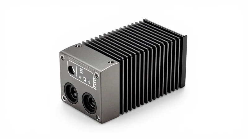
The External Laser Source (ELS) strategy is the industry's response to the 'thermal wall' encountered when integrating III-V semiconductor lasers directly onto high-power silicon photonics dies. By moving the laser—the component most sensitive to heat and most prone to failure—out of the main CPO package and into a separate, pluggable module on the front panel, engineers can optimize thermal management and significantly improve the operational lifespan of the entire networking system.
Solving the Thermal and Reliability Paradox
Laser diodes exhibit a sharp decline in efficiency and an increase in noise as temperatures rise, typically requiring a stable environment below 50-60°C for optimal performance. Conversely, modern high-radix switch ASICs can reach temperatures exceeding 100°C. Placing them in the same package creates a reliability paradox. Decoupling the laser allows it to reside in a cooler zone of the chassis, serviced by dedicated airflow and heatsinks, while the silicon photonics modulators remain tightly integrated with the ASIC to minimize electrical trace losses.
| Feature | Integrated (On-Chip) Laser | External Laser Source (ELS) |
|---|---|---|
| Thermal Exposure | High (shares ASIC heat sink) | Low (independent cooling) |
| Field Serviceability | Impossible (requires full board swap) | High (hot-pluggable modules) |
| Optical Power Loss | Minimal (direct coupling) | Higher (fiber coupling losses) |
| Laser Density | Limited by die area | Scalable via external splitting |
The Path to Standardization: OIF and ELSFP
To prevent vendor lock-in and ensure a robust ecosystem, the Optical Internetworking Forum (OIF) has been instrumental in defining the External Laser Source Form Factor (ELSFP). This standard specifies the mechanical, electrical, and optical interfaces for blind-mate pluggable modules. These modules utilize Polarization Maintaining Fiber (PMF) to deliver high-power Continuous Wave (CW) light to the CPO engines, ensuring that light sources from different manufacturers are interoperable with various CPO switch designs.
Frequently Asked Questions about ELS
- Why not use integrated lasers if they have lower optical loss?
While integrated lasers reduce coupling loss, the failure of a single laser would require discarding the entire multi-thousand-dollar CPO-switch assembly. The ELS allows for 'pay-as-you-grow' scaling and easy replacement of failed light sources without disrupting the host ASIC. - How does ELS handle polarization?
ELS modules use Polarization Maintaining Fiber (PMF) to ensure the light arriving at the silicon photonics modulators is correctly aligned, which is critical for efficient modulation. - Does moving the laser increase power consumption?
It adds a small overhead due to coupling losses (1-2 dB), but this is largely offset by the fact that lasers operate much more efficiently at lower temperatures, requiring less drive current for the same optical output.
Standardization and Ecosystem: The Role of OIF and COBO
The successful commercialization of Co-Packaged Optics (CPO) depends entirely on the industry's ability to move away from proprietary, 'black-box' solutions toward standardized, interoperable architectures. Without common mechanical, electrical, and optical interfaces, hyperscale data center operators risk vendor lock-in, which stifles innovation and increases supply chain fragility. Organizations like the Optical Internetworking Forum (OIF) and the Consortium for On-Board Optics (COBO) are the architects of this transition, defining the physical and electrical foundations that allow silicon photonics chips to coexist with switch ASICs on a single substrate.
The OIF 3.2T CPO Project and Implementation Agreements
The OIF has been instrumental in creating the 3.2T CPO Implementation Agreement (IA), which targets a 3.2 Tbps aggregate bandwidth module. This project defines the critical parameters for CPO modules used in 51.2T and future 102.4T switching platforms. Crucially, the OIF's work extends to the External Laser Source (ELS), where the Small Form Factor Pluggable (SFP) and Quad Small Form Factor Pluggable (QSFP) form factors are being adapted to serve as standardized remote light sources. By decoupling the laser from the CPO engine, the OIF addresses thermal management and reliability while ensuring that lasers from different vendors can power any CPO-enabled switch.
COBO: Driving Board-Level Innovation
While the OIF focuses heavily on electrical interfaces and module specifications, the Consortium for On-Board Optics (COBO) provides the structural framework for embedding optical engines within the printed circuit board (PCB) environment. COBO's working groups focus on the mechanical challenges of high-density interconnects, including specialized connectors and thermal interface materials. Their work ensures that as we move from pluggable optics to CPO, the physical reliability of the board-to-chip connection remains robust under the intense heat generated by modern AI and networking silicon.
| Organization | Primary Focus | Key Contribution to CPO |
|---|---|---|
| OIF | Electrical & Optical Interoperability | 3.2T CPO IA and ELSFP (External Laser Source) specifications. |
| COBO | Mechanical & Board Integration | Standards for on-board optical engine form factors and thermal pathways. |
| IEEE (802.3) | Ethernet Protocol Standards | Defining the physical layer (PHY) rates like 400GbE, 800GbE, and 1.6Te. |
The Multi-Vendor Interoperability Challenge
Interoperability is the 'Holy Grail' for CPO adoption. In a mature ecosystem, a network engineer should be able to install a CPO module from Vendor A and a remote laser source from Vendor B into a switch chassis designed by Vendor C. Standardization bodies are currently refining the 'blind mate' connectors and the management interface protocols (like CMIS) to ensure that these disparate components can communicate and initialize without manual tuning. This shift toward a common ecosystem is what will ultimately drive down the cost-per-bit and enable the mass deployment of CPO in AI scale-out fabrics.
- Why is the OIF 3.2T project important?
It provides a standardized blueprint for 3.2 Tbps optical engines, ensuring they are compatible with the next generation of high-capacity switch ASICs. - What role does the External Laser Source (ELS) play in standards?
Standards like ELSFP allow for a hot-pluggable, interchangeable laser module that sits at the front panel, simplifying maintenance and improving thermal isolation. - How does COBO complement OIF?
While OIF handles 'how it speaks' (signaling), COBO handles 'how it fits' (mechanical and thermal placement on the PCB).
Challenges to Mainstream Adoption: Reliability and Yield
The transition from pluggable transceivers to Co-Packaged Optics (CPO) represents a fundamental shift in risk management; while CPO solves the 'power wall' problem, it introduces a single-point-of-failure risk where a faulty optical component can compromise an entire high-value switch ASIC. Achieving mainstream adoption requires solving the 'Known Good Die' (KGD) challenge and establishing manufacturing yields that match the rigorous standards of the semiconductor industry.
The Known Good Die (KGD) Challenge
In the pluggable optics model, the transceiver and the switch are decoupled; if a module fails, it is swapped in seconds. With CPO, the silicon photonics engines are permanently bonded or closely coupled with the switch silicon. The KGD problem dictates that manufacturers must ensure the optical engine is 100% functional before integration. If an optical die with a 90% yield is integrated with a switch ASIC that has a 90% yield, the composite yield drops significantly, leading to the potential scrapping of extremely expensive silicon assemblies due to a failure in a relatively lower-cost optical component.
Comparative Yield Risks: Pluggables vs. CPO
| Metric | Pluggable Optics | Co-Packaged Optics (CPO) |
|---|---|---|
| Failure Impact | Replaceable module; zero system downtime. | Potential loss of entire switch/ASIC package. |
| Testing Complexity | Tested as a finished standalone unit. | Requires wafer-level and interposer-level testing. |
| Yield Sensitivity | Low; faulty units are discarded early. | High; cumulative yield loss impacts TCO. |
| Field Service | Hot-swappable by technicians. | Requires factory-level rework or replacement. |
Manufacturing Complexity and Reworkability
The assembly of CPO involves high-precision flip-chip bonding and advanced packaging techniques like TSV (Through-Silicon Vias). These processes are sensitive to thermal expansion mismatches between the organic substrate, the silicon ASIC, and the optical engine. Furthermore, the industry lacks a standardized 'rework' process. If a defect is detected post-packaging, extracting the optical engine without damaging the switch substrate is technically daunting and currently cost-prohibitive for high-volume manufacturing.
Critical Adoption FAQ
- How does CPO reliability compare to traditional optics?
While silicon photonics components themselves are highly reliable, the increased complexity of the interconnects and the thermal proximity to the ASIC introduce new failure modes that are still being characterized. - What is being done to mitigate yield loss?
Industry leaders are developing 'chiplet' architectures and standardized socketed interfaces that allow for more modular assembly, theoretically enabling the replacement of failed optical engines without scrapping the ASIC. - Is the cost of failure the biggest barrier?
Yes. Until the yield of optical engines reaches the 'six nines' level of reliability expected in data center switching, the financial risk of co-packaging remains a primary concern for hyperscalers.
The Roadmap: From Pluggable Co-Existence to Full CPO Dominance
The path to Co-Packaged Optics (CPO) dominance is characterized by a phased co-existence with pluggable form factors rather than an immediate displacement. While pluggables remain the industry workhorse for 400G and early 800G deployments, the transition begins in earnest as data centers approach 51.2T and 102.4T switching capacities, where the power density and signal integrity requirements of traditional DSP-based pluggables reach their physical and economic limits.
Phase 1: The LPO Bridge (2026–2026)
Linear Drive Pluggable Optics (LPO) serves as the intermediate step in the roadmap. By removing the power-hungry Digital Signal Processor (DSP) from the optical module and relying on the switch ASIC’s SerDes to drive the signal, LPO achieves power savings of up to 50% compared to traditional retimed pluggables. This allows the industry to extend the life of the pluggable ecosystem while solving the immediate thermal constraints of 800G and 1.6T transitions without moving to the complex manufacturing environment of CPO.
Phase 2: Hybrid Deployments and Hyperscale Adoption (2026–2028)
As switching speeds move toward 102.4T, the industry will witness the first large-scale CPO deployments, primarily within the AI/ML back-end fabrics of hyperscale data centers. In these environments, the ultra-low latency and massive bandwidth density of CPO outweigh the serviceability risks. During this phase, we expect to see 'Hybrid' racks where CPO is used for internal high-speed clustering, while traditional pluggables or LPO handle the North-South traffic to the leaf/spine network.
| Feature | Linear Drive (LPO) | Co-Packaged Optics (CPO) |
|---|---|---|
| Typical Era | 51.2T Switch Generation | 102.4T+ Switch Generation |
| Power Efficiency | Moderate (DSP-free) | Maximum (Proximity-based) |
| Serviceability | High (Field Replaceable) | Low (Integrated into ASIC) |
| Primary Use Case | General Cloud Networking | AI/ML Clusters & HPC |
| Ecosystem | Mature / Multi-vendor | Emerging / ELSFP focused |
Phase 3: The 200T Era and Full CPO Dominance (2029+)
Beyond 2028, as the industry eyes 204.8T switching capacities, the electrical 'reach' between the switch ASIC and the front panel becomes nearly impossible to maintain with copper or even advanced LPO. At this stage, CPO becomes the default architecture. Standardized External Laser Sources (ELSFP) will have solved the thermal and reliability concerns of the early 2020s, enabling a robust multi-vendor ecosystem that mirrors the flexibility once offered by pluggable modules.
- Will CPO completely kill the pluggable market?
Unlikely in the near term. Pluggables will remain the standard for enterprise and edge networking where power density is less critical and field serviceability is a priority. - What is the biggest catalyst for the switch to CPO?
The exponential growth of AI training clusters, which require massive bandwidth with the lowest possible latency and power consumption. - Is the industry currently favoring LPO or CPO?
Current momentum favors LPO for the 800G cycle because it uses existing manufacturing infrastructure, but CPO is viewed as the inevitable long-term solution for 1.6T and 3.2T per-port speeds.
Co-Packaged Optics is no longer a research concept; it is a mandatory evolution for the next decade of hyper-scale networking. While hurdles in manufacturing and serviceability remain, the power-saving benefits make CPO inevitable for 1.6T and 3.2T generations. To stay ahead of the curve in data center architecture, organizations must begin evaluating their silicon photonics roadmap today. Contact our engineering team for a consultation on future-proofing your optical network.