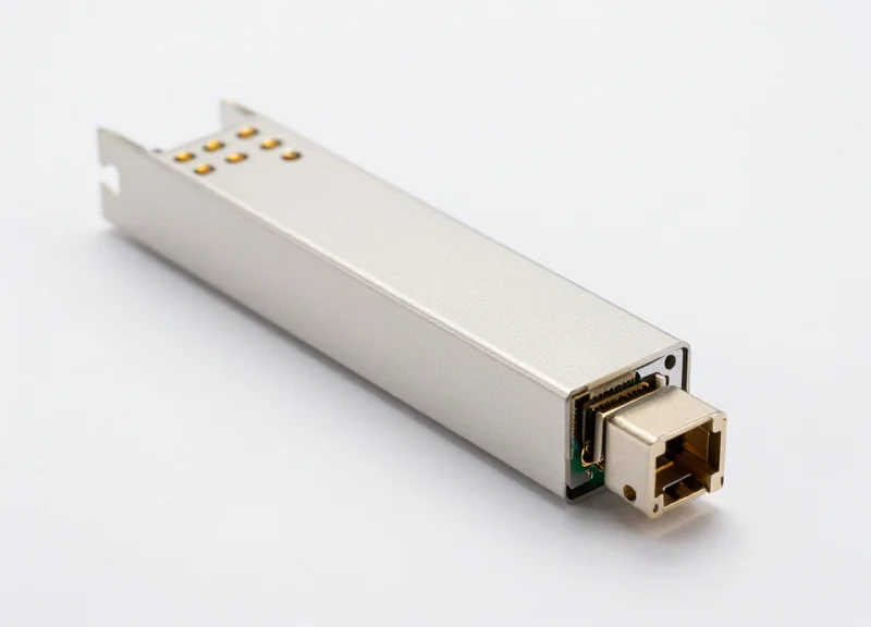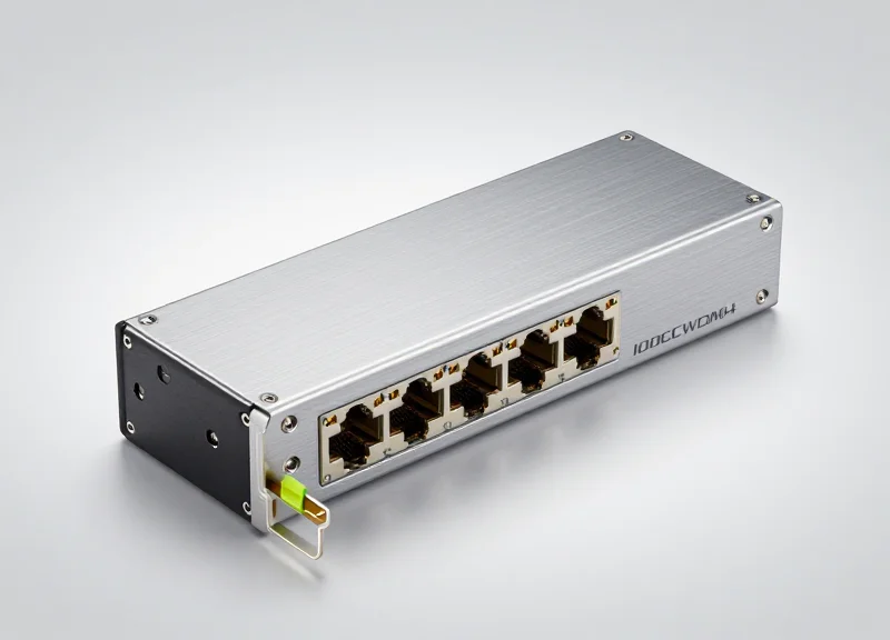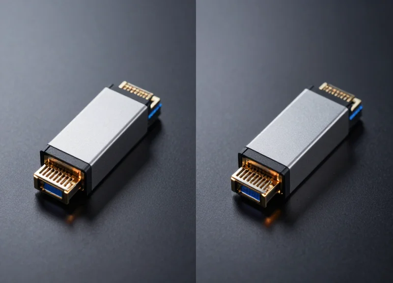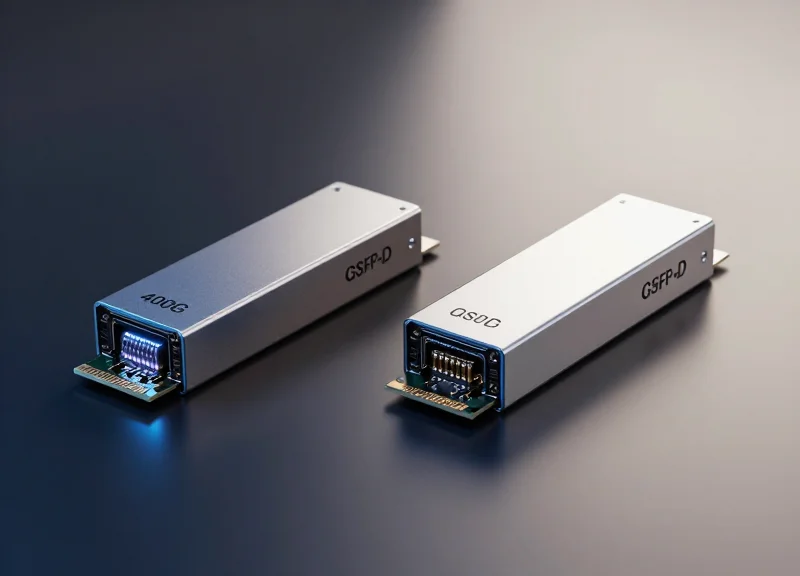
As data centers transition to 400G and beyond to support AI and high-performance computing, the choice of optical engine determines the limits of scalability and sustainability. This guide evaluates Silicon Photonics against traditional standards to help network architects optimize for efficiency, reliability, and cost.
The Evolution of 400G Connectivity

The Evolution of 400G Connectivity
The shift to 400G connectivity marks a pivotal transition in data center architecture, moving away from simple bandwidth scaling toward highly integrated, power-efficient optical engines. While legacy 100G solutions relied heavily on discrete components like Directly Modulated Lasers (DML) and Electro-absorption Modulated Lasers (EML), the 400G era leverages Silicon Photonics (SiPh) to overcome the physical and economic limitations of traditional indium phosphide-based optics. This evolution is driven by the need for higher port density and lower cost-per-bit, positioning silicon photonics not just as an alternative, but as a primary enabler of the next generation of networking.
The Catalyst: Hyperscale and AI Demands
The primary catalyst for 400G adoption is the explosive growth of Artificial Intelligence (AI) and Machine Learning (ML) clusters, which require massive East-West traffic throughput. Traditional optical modules struggle with the thermal and spatial constraints of high-density switch environments. Silicon photonics addresses these challenges by integrating multiple optical functions onto a single silicon chip using CMOS-compatible processes, significantly reducing the footprint and manufacturing complexity compared to legacy discrete assemblies.
| Feature | Legacy 100G Architecture | Modern 400G Architecture (SiPh) |
|---|---|---|
| Modulation Scheme | NRZ (Non-Return to Zero) | PAM4 (Pulse Amplitude Modulation) |
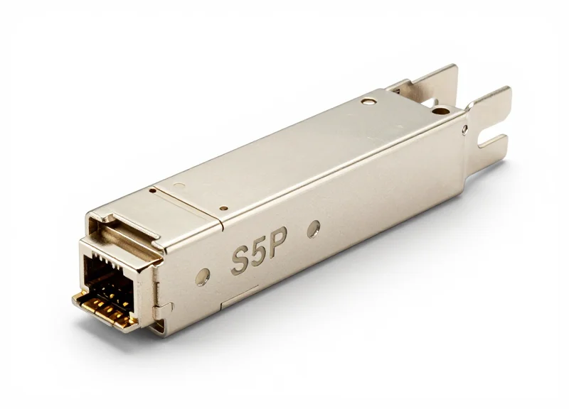
| Form Factor | QSFP28 | QSFP-DD / OSFP |
| Component Integration | Discrete Components | Monolithic/Hybrid Integration |
| Typical Reach | Up to 10km | Up to 2km (DR4) / 10km (FR4) |
Technological Transitions: From Discrete to Integrated
In the legacy era, increasing bandwidth meant adding more physical lasers and fibers, which hit a ceiling in terms of power consumption and physical space. The evolution to 400G introduced PAM4 modulation, which effectively doubles the data rate per symbol. However, PAM4 is more sensitive to noise, requiring the high-signal integrity provided by the precise waveguides found in silicon photonics. This technological shift allows operators to scale from 12.8Tbps switches to 25.6Tbps and 51.2Tbps generations without a linear increase in power requirements.
Common Questions on the 400G Transition
- Why is 400G preferred over multi-lane 100G?
400G offers significantly better power efficiency per gigabit and higher port density, which reduces the Total Cost of Ownership (TCO) for large-scale data centers compared to stacking multiple 100G links. - What role does PAM4 play in this evolution?
PAM4 modulation is the foundation of 400G, allowing for 50G or 100G per-lane speeds. This reduces the number of optical components needed to reach 400G total throughput. - How does Silicon Photonics lower manufacturing costs?
By utilizing existing CMOS semiconductor fabrication plants, SiPh allows for high-volume automated wafer-level testing and packaging, which is far more scalable than the manual assembly required for discrete optics.
Decoding Silicon Photonics (SiPh) vs. EML and VCSEL
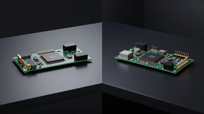
The choice between Silicon Photonics (SiPh), Electro-absorption Modulated Lasers (EML), and Vertical-Cavity Surface-Emitting Lasers (VCSEL) for 400G infrastructure is fundamentally a trade-off between transmission distance, integration density, and cost-per-bit. While VCSEL remains the incumbent for short-reach multi-mode applications, SiPh and EML represent a critical divergence in how light is modulated and transmitted over single-mode fiber, with SiPh leveraging CMOS manufacturing for high-density integration and EML providing superior signal integrity for long-distance 400G connectivity.
Architectural Breakdown: Material Science and Light Modulation
At the 400G level, the physical mechanism of light generation and modulation differs significantly across these three technologies. VCSELs are multi-mode Gallium Arsenide (GaAs) based lasers that emit light perpendicular to the chip surface. They are inexpensive and power-efficient but suffer from limited bandwidth and high chromatic dispersion, restricting their use to short-reach (SR) links. EMLs, conversely, integrate an Indium Phosphide (InP) laser diode with an electro-absorption modulator on a single chip. This configuration minimizes 'chirp' (wavelength shifts during modulation), making EML the gold standard for 400G-FR4 and LR4 applications where signal clarity over 2km to 10km is paramount.
Silicon Photonics departs from these traditional 'all-in-one' laser designs. In a SiPh architecture, the laser source is often external (using a Continuous Wave laser), while the modulation and waveguiding are performed on a silicon-on-insulator (SOI) substrate. By using Mach-Zehnder Modulators (MZM) or Micro-ring Resonators (MRR) etched directly into the silicon, SiPh can achieve high-speed PAM4 signaling while utilizing existing semiconductor fabrication plants, significantly reducing the cost of high-volume production for 400G-DR4 modules.
| Feature | VCSEL | EML | Silicon Photonics (SiPh) |
|---|---|---|---|
| Material Base | GaAs (Gallium Arsenide) | InP (Indium Phosphide) | SOI (Silicon-on-Insulator) |
| Max Reach (400G) | ~100m (Multi-mode) | 2km - 10km (Single-mode) | 500m - 2km (Single-mode) |
| Modulation Type | Direct Modulation | Integrated Absorption | External Mach-Zehnder |
| Manufacturing Scalability | High | Low to Moderate | Very High (CMOS) |
| Power Consumption | Lowest | Moderate to High | Moderate |
Performance Trade-offs in 400G Deployments
When deploying 400G in data centers, the decision often hinges on the 'Yield vs. Performance' curve. EML-based transceivers provide the best Optical Modulation Amplitude (OMA) and Extinction Ratio, ensuring low Bit Error Rates (BER) over longer fiber runs. However, EML manufacturing involves complex III-V wafer processing, which typically results in lower yields and higher unit costs. Silicon Photonics offers a 'middle ground' for 400G-DR4 (500m) links; it provides higher reliability due to fewer discrete components and a path toward co-packaged optics (CPO) where the optics are integrated directly with the switch ASIC.
Technical Comparison FAQ
- Why is VCSEL limited to 100 meters at 400G?
VCSELs operate on multi-mode fiber which suffers from modal dispersion. At 400G speeds (using 53Gbd PAM4), the signal integrity degrades rapidly after 70-100 meters, making it unsuitable for spine-to-leaf connections. - Does Silicon Photonics require a separate laser?
Yes. Silicon itself is an inefficient light emitter due to its indirect bandgap. Therefore, SiPh modules require an external InP-based laser source (the 'light bulb') which is then coupled into the silicon chip for modulation. - Which technology is better for 400G-FR4 (2km)?
Currently, EML is the dominant technology for FR4 due to its superior power budget and lower insertion loss compared to early-generation SiPh MZMs, though SiPh is rapidly closing the gap.
Latency Benchmarks: Impact on Real-Time Applications
Latency Benchmarks: Impact on Real-Time Applications
In the realm of 400G connectivity, latency is primarily dictated by the modulation scheme and the necessary Digital Signal Processing (DSP) rather than the optical material itself. Silicon Photonics (SiPh) and Electro-absorption Modulated Lasers (EML) both utilize PAM4 modulation at 400G, which introduces a baseline latency of approximately 100ns to 150ns due to Forward Error Correction (FEC). However, Silicon Photonics offers an architectural advantage through tighter integration; by moving the optical engine closer to the ASIC, the electrical trace length is minimized, reducing signal degradation and transmission time at the nanosecond scale.
Comparative Latency Breakdown
While the speed of light through fiber remains constant, the 'time-to-glass'—the duration it takes for an electrical signal to be converted to optical—varies based on the driver circuitry and the physical layout of the transceiver. Silicon Photonics typically mirrors the performance of EMLs but significantly outperforms VCSELs in long-reach scenarios where signal re-retiming is mandatory.
| Technology | Modulation | Avg. Transceiver Latency | Primary Latency Source |
|---|---|---|---|
| Silicon Photonics (SiPh) | PAM4 | <10ns (excluding DSP) | Modulator Driver & Waveguide |
| EML (InP) | PAM4 | <10ns (excluding DSP) | Thermal Stabilization (TEC) |
| VCSEL | NRZ/PAM4 | <5ns (excluding DSP) | Laser Relaxation Oscillation |
Workload Analysis: AI Training and HFT
For AI and Machine Learning (ML) workloads, latency is a compounding factor. In large-scale GPU clusters using RDMA (Remote Direct Memory Access), any delay in the 400G fabric slows down the synchronization of gradients across nodes. Silicon Photonics is increasingly preferred here not just for its latency parity, but for its reliability at scale, which prevents 'tail latency' spikes caused by intermittent signal errors. In High-Frequency Trading (HFT), where every nanosecond counts, the industry is exploring 'DSP-lite' or LPO (Linear Drive Pluggable Optics) versions of Silicon Photonics to bypass the 100ns+ FEC delay entirely.
- Does Silicon Photonics have higher latency than traditional EML?
No, at the 400G standard, both SiPh and EML exhibit nearly identical latency profiles because the bottleneck is the DSP-based PAM4 processing, not the optical emission. - How does FEC impact real-time 400G applications?
Forward Error Correction adds roughly 100ns of latency to ensure data integrity. For real-time applications like HFT, engineers often seek low-latency FEC algorithms or direct-drive optics. - Why is Silicon Photonics considered 'future-proof' for low-latency needs?
SiPh allows for Co-Packaged Optics (CPO), which places the optical interface on the same substrate as the processor, potentially eliminating centimeters of electrical PCB traces and reducing latency further.
Power Consumption: The Energy Efficiency Gap
At the 400G threshold, Silicon Photonics (SiPh) establishes a decisive energy efficiency lead by consolidating optical modulation and detection onto a single CMOS-compatible die, typically consuming between 8W and 10W per module. This represents a 15% to 20% reduction in power consumption compared to traditional Electro-absorption Modulated Laser (EML) solutions, which often exceed 12W due to the thermal overhead of discrete components and complex driver requirements.
Quantifying the Efficiency: Milliwatts per Gigabit
The primary metric for evaluating optical efficiency in the data center is milliwatts per gigabit (mW/Gbps). As data rates climb, the energy required to maintain signal integrity over distance becomes a limiting factor for rack density.
| Technology Type | Typical 400G Power (W) | Efficiency (mW/Gbps) | Transmission Reach |
|---|---|---|---|
| Silicon Photonics (SiPh) | 8.0 - 10.0 | 20.0 - 25.0 | Up to 2km (DR4/DR4+) |
| EML (Discrete) | 10.0 - 12.5 | 25.0 - 31.2 | Up to 10km (LR4/FR4) |
| VCSEL (Multimode) | 7.5 - 9.0 | 18.7 - 22.5 | Up to 100m (SR8) |
Thermal Dissipation and Cooling Requirements
Higher power consumption does not just increase electricity bills; it creates a cascade of thermal management challenges. EML-based transceivers generate concentrated heat that requires aggressive cooling strategies, often necessitating higher fan speeds and more robust airflow management within the switch chassis. Silicon Photonics, by contrast, leverages a more distributed thermal profile. Because the laser source (often an external or integrated DFB) can be decoupled from the high-speed modulator, heat is easier to dissipate, allowing for higher port density without exceeding the thermal envelope of the QSFP-DD or OSFP form factors.
The Carbon Footprint of Hyperscale Connectivity
For a data center deploying tens of thousands of 400G links, the cumulative savings of SiPh are substantial. A 2W saving per module across 50,000 links equates to 100kW of constant load reduction. When factoring in the Power Usage Effectiveness (PUE) of the facility, the total energy reduction at the utility level can double, directly contributing to corporate sustainability goals and reducing the overall carbon footprint of AI and cloud operations.
FAQ: Power and Energy Efficiency
- Does Silicon Photonics always consume less power than VCSEL?
No. VCSEL technology remains more power-efficient for short-reach, multimode applications (under 100 meters). However, for single-mode fiber reaches required in modern leaf-spine architectures, SiPh is significantly more efficient than EML alternatives. - How does SiPh improve reliability through power management?
Lower power consumption leads to lower operating temperatures. Since the failure rate of optoelectronic components is thermally sensitive, the reduced heat output of SiPh modules generally correlates to a higher Mean Time Between Failures (MTBF). - Will the energy gap widen at 800G and 1.6T?
Yes. As speeds double, the power penalty for discrete EML designs grows non-linearly. Silicon Photonics is expected to be the primary vehicle for Co-Packaged Optics (CPO), which will further reduce power by moving the optical engine closer to the switch ASIC.
Total Cost of Ownership (TCO) Deep Dive
Total Cost of Ownership (TCO) Deep Dive
The Total Cost of Ownership for 400G Silicon Photonics (SiPh) is characterized by a superior long-term value proposition where the high initial investment in design is offset by the massive scalability of CMOS-based manufacturing and significantly lower power-related operational expenses. While traditional EML-based solutions offer mature yields today, Silicon Photonics provides a more predictable cost reduction curve as data centers migrate toward 800G and beyond.
CapEx: From Discrete Assembly to Wafer-Scale Integration
Capital Expenditure in 400G networks is heavily influenced by the manufacturing methodology. Traditional transceivers rely on discrete components—lasers, modulators, and detectors—that must be individually aligned and tested. In contrast, Silicon Photonics enables thousands of optical circuits to be fabricated on a single 300mm silicon-on-insulator (SOI) wafer. This 'wafer-scale' approach reduces the physical footprint and the number of bill-of-material (BOM) components, although the cost of integrating the initial light source (InP laser) remains a significant factor.
| Cost Driver | Silicon Photonics (SiPh) | EML (Traditional) | VCSEL (Short Reach) |
|---|---|---|---|
| Manufacturing | CMOS / Wafer-Scale | Discrete Compound Semi | Wafer-Level Batch |
| BOM Complexity | Low (Integrated) | High (Multi-part) | Medium |
| Testing Cost | Low (Wafer-level) | High (Individual) | Moderate |
| Relative CapEx | Moderate to High | High | Low |
OpEx: Energy Efficiency and Thermal Reliability
Operational Expenditure is where Silicon Photonics demonstrates its primary advantage. In a hyperscale environment, energy consumption accounts for nearly 40% of the total OpEx. SiPh modulators, particularly those utilizing advanced MZI (Mach-Zehnder Interferometer) designs, can operate with higher thermal tolerance than EML counterparts. This stability reduces the burden on data center cooling systems and allows for higher density rack configurations without exceeding the thermal envelope of the chassis.
Manufacturing Yields and Maturity
The primary challenge to SiPh TCO remains the 'yield gap.' Because SiPh involves complex integration of non-native materials like Indium Phosphide for lasers, initial production batches may have lower yields than the highly mature EML processes. However, once a SiPh process reaches maturity, the marginal cost of producing an additional unit is significantly lower than traditional methods, making it the more economical choice for high-volume deployments exceeding 100,000 units.
- Does Silicon Photonics require higher upfront investment?
Yes, the design and tape-out costs for SiPh are higher due to the semiconductor-grade masks required, but the per-unit cost drops faster than EML as volume increases. - How does reliability impact TCO?
SiPh offers higher Mean Time Between Failures (MTBF) because it reduces the number of discrete solder points and manual alignments, lowering maintenance costs. - Is SiPh cost-effective for all distances?
SiPh is most cost-effective for 400G-DR4 (500m to 2km) and above. For very short reaches (under 100m), VCSEL technology remains the cheaper alternative.
Reliability and Thermal Stability at High Density
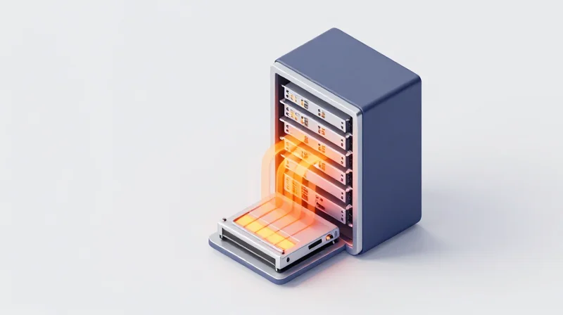
Thermal Stability: The Crucial Reliability Factor for 400G
In the transition to 400G and 800G architectures, thermal management becomes the primary bottleneck for network uptime and hardware longevity. Silicon Photonics (SiPh) inherently addresses this by utilizing silicon substrates which possess a thermal conductivity of approximately 149 W/m·K—nearly double that of Indium Phosphide (InP), the material used in most alternative 400G lasers. This allows SiPh-based transceivers to dissipate heat more efficiently across the optical engine, preventing the localized 'hot spots' that typically lead to wavelength drift and accelerated component failure in traditional Electro-absorption Modulated Lasers (EML).
Material Performance and Thermal Metrics
| Thermal Property | Silicon Photonics (SiPh) | Indium Phosphide (InP/EML) |
|---|---|---|
| Thermal Conductivity | 149 W/m·K (Superior Heat Sink) | 68 W/m·K (Insulating Behavior) |
| Wavelength Stability | High (Passive Waveguides) | Low (Temperature Dependent) |
| Laser Configuration | Can use External Laser Sources (ELS) | Integrated (High Thermal Stress) |
| Max Operating Temp | Up to 85°C without active cooling | Requires Thermo-Electric Cooling (TEC) |
Decoupling Heat from Modulation
One of the most significant reliability advantages of Silicon Photonics in 400G environments is the ability to decouple the light source from the electronic heat zone. Traditional 400G optics integrate the laser directly onto the hot ASIC-adjacent area, subjecting it to extreme thermal cycling. Silicon Photonics enables the 'External Laser Source' (ELS) architecture, where the heat-sensitive laser can be placed in a cooler, separate part of the module or even a different chassis location. This separation drastically reduces the Mean Time Between Failures (MTBF) and ensures that the optical signal remains stable even as the switch density increases.
Thermal Reliability FAQ
- Does heat increase the Bit Error Rate (BER) in 400G modules?
Yes, in traditional EML-based alternatives, high temperatures cause wavelength shifting which increases signal jitter and BER. SiPh maintains a more consistent refractive index across temperature ranges, ensuring a stable BER. - Why is Silicon Photonics considered more reliable for AI clusters?
AI clusters run at near-constant 100% load, generating sustained high temperatures. SiPh transceivers handle this load better because their passive components do not degrade under heat as quickly as active InP components. - How does SiPh reduce cooling costs?
By operating efficiently at higher temperatures without the need for power-hungry Thermo-Electric Coolers (TECs), SiPh modules reduce the overall energy required for data center climate control.
Manufacturing Scale: The CMOS Advantage

The CMOS Advantage in Optical Fabrication
Silicon Photonics (SiPh) fundamentally changes the economics of 400G networking by shifting optical production from a specialized boutique process to a high-volume semiconductor workflow. By utilizing standard 300mm silicon-on-insulator (SOI) wafers and existing Deep Ultraviolet (DUV) lithography, SiPh enables the integration of complex optical functions—such as modulators, splitters, and detectors—directly onto a single silicon die. This compatibility with the massive CMOS (Complementary Metal-Oxide-Semiconductor) ecosystem allows manufacturers to bypass the manual, labor-intensive alignment processes required for traditional Indium Phosphide (InP) or discrete optics, resulting in superior quality control and rapid volume scaling.
Comparing Production Ecosystems
| Manufacturing Factor | Silicon Photonics (SiPh) | Traditional III-V (InP/EML) |
|---|---|---|
| Wafer Diameter | 200mm - 300mm (High Capacity) | 2-inch - 6-inch (Limited Capacity) |
| Tooling Infrastructure | Standard Semiconductor Foundries | Specialized Compound Foundries |
| Integration Type | Monolithic / Large Scale | Discrete / Hybrid Assembly |
| Testing Workflow | Automated Wafer-Level Testing | Post-Dicing Component Testing |
| Cost Curve | Aggressive reduction with volume | Linear reduction; limited by labor |
Automated Wafer-Level Reliability
A critical yield advantage for Silicon Photonics is the ability to perform high-speed automated optical testing while components are still in wafer form. In traditional 400G manufacturing, optical performance is often verified only after the chip has been diced and partially assembled into expensive sub-modules. SiPh allows for 'fail-fast' diagnostics, where thousands of optical circuits are probed simultaneously. This ensures that only Known Good Dies (KGD) move forward into the packaging phase, drastically reducing waste and ensuring that the final 400G transceivers meet stringent reliability standards for hyperscale data centers.
Manufacturing Scale FAQ
- Does Silicon Photonics require custom fabrication plants?
No, one of its greatest strengths is that it can be manufactured in existing commercial CMOS foundries like TSMC or GlobalFoundries, leveraging trillions of dollars in existing R&D and equipment. - How does wafer size impact the final price of 400G modules?
Moving from the 2-inch or 4-inch wafers used in III-V materials to 300mm silicon wafers increases the number of chips per wafer by orders of magnitude, slashing the per-unit fixed costs. - Is the reliability of CMOS-based optics comparable to traditional methods?
Yes, and often superior. Because the processes are highly automated and standardized, there is significantly less variance between batches compared to manual assembly techniques.
Future-Proofing: Path to 800G and 1.6T
The Scalability Challenge: Moving Beyond 400G
Silicon Photonics (SiPh) represents the most viable architectural foundation for 800G and 1.6T networks because it facilitates the inevitable transition from traditional pluggable modules to Co-Packaged Optics (CPO). As lane rates move toward 200G, the physical limitations of discrete Electro-absorption Modulated Lasers (EML) regarding power density and thermal management become increasingly prohibitive, whereas SiPh's ability to integrate high-speed modulators with CMOS electronics provides a scalable, lower-power alternative for high-density environments.
Technological Roadmap: SiPh vs. Alternatives
| Metric | Silicon Photonics (SiPh) | EML (InP) | Thin-Film Lithium Niobate (TFLN) |
|---|---|---|---|
| Max Lane Rate | 200G - 400G per lane | 200G (challenging) | 400G+ (experimental) |
| Integration Type | Monolithic / CPO-ready | Discrete Pluggable | Hybrid / Heterogeneous |
| Power Efficiency | High (Lowest pJ/bit in CPO) | Low (High thermal load) | High (Low drive voltage) |
| Manufacturing Scale | CMOS Foundries (Mature) | Specialized InP Fabs | Low (Scaling phase) |
The Role of Co-Packaged Optics (CPO) in 1.6T Evolution
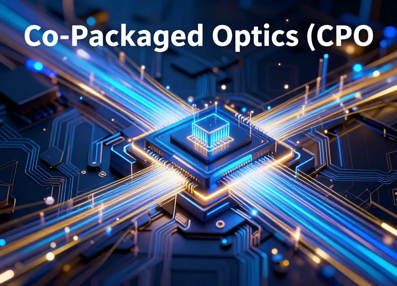
At 1.6T, the signal integrity requirements of electrical traces between the Switch ASIC and the optical engine become a major bottleneck. Silicon Photonics is uniquely suited for CPO, where the optical engine is moved onto the same substrate as the ASIC. This proximity reduces trace length and eliminates the need for power-hungry Retimers. While Thin-Film Lithium Niobate (TFLN) offers superior modulation bandwidth, SiPh's compatibility with existing high-volume silicon manufacturing ensures it remains the primary platform for 800G deployment and the bridge to 1.6T CPO solutions.
- Why is 200G per lane critical for future-proofing?
200G per lane is the fundamental building block for 800G (4 lanes) and 1.6T (8 lanes). Silicon Photonics modulators are currently the only technology that can be manufactured at scale to support these rates while keeping power consumption within the thermal envelope of modern data centers. - Can traditional EML scale to 1.6T?
While technically possible, EML requires significantly more power and complex cooling as bandwidth increases. At 1.6T, the cost and heat generated by an EML-based solution would likely exceed the operational budget of most hyperscale facilities. - What is the primary risk for Silicon Photonics in this roadmap?
The main challenge is maintaining low insertion loss as complexity increases. However, the industry is mitigating this through advanced laser integration techniques and hybrid bonding, ensuring SiPh remains the most competitive path forward.
While traditional EML and VCSEL solutions still hold value in specific niches, Silicon Photonics is emerging as the superior choice for scalable, high-efficiency 400G deployments. To determine the best fit for your infrastructure, consult with our optical engineering experts today for a detailed performance audit.