As data demands skyrocket driven by AI and cloud computing, traditional optical transceivers are hitting physical and economic limits. Silicon Photonics (SiPh) emerges as the transformative solution, integrating complex optical functions onto a silicon chip using standard CMOS processes. This guide dives into the mechanics of 400G Silicon Photonics and why it is becoming the backbone of modern high-speed networks.
The Fundamentals of Silicon Photonics Technology

The Fundamentals of Silicon Photonics Technology
Silicon photonics is a transformative technology that integrates laser-based optical communication into the silicon-based microchips that power modern electronics. By utilizing the same Complementary Metal-Oxide-Semiconductor (CMOS) fabrication processes used for microprocessors and memory chips, silicon photonics enables the manipulation of photons rather than electrons as the primary carrier of information. This hybrid approach overcomes the physical limitations of copper-based electrical signals, which suffer from high attenuation and thermal dissipation at the ultra-high frequencies required for 400G and 800G networking.
The Convergence of Optics and Semiconductors
The core innovation lies in the use of silicon as an optical waveguide. Because silicon is transparent at the infrared wavelengths (typically 1310nm and 1550nm) used in fiber-optic communications, it can be etched into microscopic channels that direct light across a chip. This integration allows for the consolidation of various discrete optical components—such as modulators, splitters, and photodetectors—directly onto a single silicon substrate. This reduces the footprint of optical transceivers and significantly lowers the cost of manufacturing through economies of scale.
| Feature | Traditional Discrete Optics | Silicon Photonics |
|---|---|---|
| Material Base | III-V Semiconductors (InP, GaAs) | Silicon on Insulator (SOI) |
| Manufacturing | Manual or semi-automated assembly | Automated CMOS foundries |
| Integration | Multiple discrete components | Monolithic or 2.5D/3D integration |
| Form Factor | Bulkier, limited by assembly | Highly miniaturized/High density |
| Cost Profile | High per-unit assembly cost | Low marginal cost at high volume |
Common Questions on Silicon Photonics Foundations
- Why use silicon if it cannot emit light efficiently?
Silicon is an indirect bandgap material, meaning it cannot serve as a laser source. However, silicon photonics sidesteps this by using 'hybrid integration' where an external Indium Phosphide (InP) laser is either bonded to the silicon wafer or coupled via a fiber, while the silicon handles the complex routing and modulation. - What is the primary advantage for 400G networks?
As data rates reach 400G, the energy required to push electrons through copper traces becomes prohibitive. Silicon photonics reduces power consumption by moving the optical conversion closer to the switch ASIC, minimizing electrical loss. - How does CMOS compatibility benefit the industry?
It allows optical components to be manufactured in existing multi-billion dollar semiconductor fabs, ensuring high yields, extreme precision, and the ability to scale production to millions of units rapidly.
In essence, silicon photonics serves as the bridge between the high-capacity world of fiber optics and the high-density world of silicon electronics. By mastering the behavior of light within a semiconductor environment, engineers can create the compact, high-bandwidth interconnects necessary for the next generation of hyperscale data centers and AI clusters.
Why 400G? The Need for Massive Bandwidth
The transition to 400G is necessitated by the exhaustion of existing 100G bandwidth capacities in environments where data processing and transmission speeds must match the rapid growth of distributed computing and high-definition content delivery. As data centers evolve, 400G becomes the critical threshold for maintaining throughput without exponentially increasing the physical footprint or power budget of the network infrastructure.
Hyperscale Expansion and East-West Traffic
Hyperscale data centers have moved away from traditional hierarchical models toward leaf-spine architectures. This shift prioritizes 'East-West' traffic—data moving between servers within the same data center—rather than 'North-South' traffic between the data center and the outside world. This internal traffic can account for up to 70% of total data center bandwidth, creating a massive bottleneck that legacy 100G interconnects can no longer support efficiently.
AI and Machine Learning Workloads
Artificial Intelligence (AI) and Machine Learning (ML) are the most significant catalysts for 400G and 800G technology. Training large language models (LLMs) requires massive GPU clusters to work in parallel, exchanging terabytes of parameter data in real-time. If the network cannot handle this synchronization at high speeds, the expensive GPUs sit idle, wasting power and increasing time-to-market. Silicon photonics enables 400G modules that offer the low latency and high reliability required for these specialized computing environments.
| Feature | 100G (Legacy) | 400G (Standard) |
|---|---|---|
| Typical Reach | Up to 10km (LR4) | 2km - 10km (FR4/LR4) |
| Modulation | NRZ | PAM4 |
| Power Efficiency | Higher W per Gbps | Significantly lower W per Gbps |
| Primary Interface | QSFP28 | QSFP-DD / OSFP |
| Bandwidth Density | Moderate | 4x Higher per Rack Unit |
Market Dynamics and Efficiency
- Why skip 200G and go straight to 400G?
While 200G was an option, many providers opted for 400G because it offered a more favorable return on investment (ROI) by doubling the capacity again with similar power and space requirements. - How does 400G help with sustainability?
400G silicon photonics modules use advanced modulation and integrated optical components to reduce the total energy consumed for every gigabit of data transmitted, helping data centers meet carbon footprint goals. - Is 400G compatible with existing fiber?
Yes, most 400G standards utilize existing Single Mode Fiber (SMF) or Multi-Mode Fiber (MMF) infrastructure, though the transceivers and switching hardware must be upgraded to support the new speeds.
Technical Architecture of 400G SiPh Transceivers
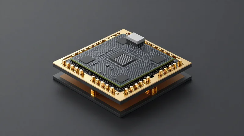
The technical architecture of a 400G Silicon Photonics (SiPh) transceiver is defined by the large-scale integration of photonic circuits onto a silicon-on-insulator (SOI) platform, effectively turning traditional discrete optical systems into integrated circuits (ICs). This architecture allows for the consolidation of modulators, photodetectors, and passive optical networks on a single die, drastically reducing the physical size of the optical engine while maintaining the high signal integrity necessary for 400Gbps transmission using PAM4 signaling.
Mach-Zehnder Modulators (MZM) and PAM4 Encoding
The primary mechanism for high-speed data encoding in 400G SiPh modules is the Mach-Zehnder Modulator. Unlike traditional lithium niobate modulators, silicon MZMs utilize the plasma dispersion effect, where the movement of free carriers (electrons and holes) within the silicon waveguide alters the refractive index. By splitting a laser beam into two arms and applying an electrical phase shift to one, the modulator creates constructive or destructive interference at the output. For 400G, these modulators typically operate across four lanes at 53.125 GBaud, utilizing Pulse Amplitude Modulation (PAM4) to achieve the required bit rate.
Germanium-on-Silicon Photodetectors
On the receiving end, the conversion of light back into electrical data is handled by Germanium-on-Silicon (Ge-on-Si) photodetectors. Since pure silicon is transparent at 1310nm and 1550nm wavelengths, germanium—a material with a smaller bandgap—is grown epitaxially onto the silicon substrate. This hybrid structure allows for high responsivity and high-speed operation, often exceeding 50GHz bandwidth, which is essential for decoding high-baud-rate 400G signals.
Architectural Comparison: SiPh vs. Traditional Optics
| Feature | Silicon Photonics (SiPh) | Traditional InP Optics |
|---|---|---|
| Integration Level | High (Monolithic IC) | Moderate (Discrete TOSA) |
| Manufacturing | CMOS Compatible | Specialized III-V Foundry |
| Modulator Type | Silicon MZM | Electro-Absorption (EAM) |
| Footprint | Highly Compact | Larger Component Size |
The Laser Integration Dilemma
A critical aspect of 400G SiPh architecture is the light source. Because silicon lacks an efficient light-emitting bandgap, manufacturers employ two main strategies: Flip-chip bonding, where an InP laser is mounted directly onto the SiPh die, or the External Laser Source (ELS) approach. The ELS configuration is gaining traction in Co-Packaged Optics (CPO) designs, as it keeps the heat-generating laser separate from the dense processing electronics, improving the overall reliability and thermal management of the 400G system.
- Why is Silicon Photonics preferred for 400G over traditional optics?
SiPh offers superior scalability and lower costs at high volumes because it leverages existing CMOS manufacturing infrastructure, allowing for higher density than discrete optics. - What is the role of the Waveguide in this architecture?
Silicon waveguides act as the 'wiring' for light, using high refractive index contrast to confine and direct light across the chip with minimal loss.
Comparing Silicon Photonics vs. Traditional InP and VCSEL
Comparing Silicon Photonics vs. Traditional InP and VCSEL
The choice between Silicon Photonics (SiPh), Indium Phosphide (InP), and Vertical-Cavity Surface-Emitting Lasers (VCSEL) for 400G applications is determined by a critical balance of reach, thermal efficiency, and manufacturing scale. While VCSELs dominate the ultra-short-reach multi-mode fiber (MMF) market and InP remains the gold standard for high-performance long-haul coherent optics, Silicon Photonics has emerged as the most disruptive force in the 500m to 2km single-mode fiber (SMF) range, offering a path to massive density at a lower cost-per-bit.
| Feature | VCSEL (GaAs) | Silicon Photonics (SiPh) | Indium Phosphide (InP) |
|---|---|---|---|
| Typical Reach | <100m (Multi-mode) | 500m - 2km (Single-mode) | 10km - 80km+ (Single-mode) |
| Bandwidth Density | Low to Medium | High (CMOS Integration) | Medium to High |
| Power Efficiency | Excellent | Good | Moderate |
| Scalability | Low (Discrete) | Excellent (Wafer-scale) | Moderate (Specialized Fab) |
| Cost at 400G | Lowest (Short Reach) | Disruptive (Mid-Reach) | Premium (Long Reach) |
The Economic and Technical Shift to SiPh
For 400G-DR4 and FR4 specifications, Silicon Photonics provides a distinct advantage through integration. Traditional InP solutions require discrete assembly of lasers, modulators, and photodetectors, which introduces significant alignment challenges and 'touch labor' costs. In contrast, SiPh leverages existing CMOS foundries to integrate everything except the light source onto a single chip. This allows for automated, wafer-level testing and high-yield manufacturing that mimics the cost curve of the microelectronics industry.
However, SiPh is not a total replacement for InP. Because silicon has an indirect bandgap, it cannot emit light efficiently. Most 400G SiPh transceivers still rely on an InP-based laser, either integrated via flip-chip bonding or coupled externally. The competition is thus less about replacing InP entirely and more about moving the complex modulation and multiplexing functions from expensive InP substrates onto cheaper, larger silicon wafers.
- Why can't VCSELs handle 400G across the data center?
VCSELs are limited by modal dispersion in multi-mode fiber and restricted modulation bandwidth. While they are efficient for top-of-rack links, they cannot maintain signal integrity over the 500m+ distances required for large-scale leaf-spine architectures. - Is InP still relevant for 400G?
Yes. InP is essential for 400G-LR8 and 400G-ZR modules. Its superior electro-optic coefficient allows for higher output power and better signal-to-noise ratios, which are necessary to overcome the attenuation of fiber links exceeding 10 kilometers. - How does Silicon Photonics improve reliability?
By reducing the number of discrete components and fiber couplings, SiPh minimizes potential points of failure and thermal sensitivity, which is critical for the high-density environments of AI clusters.
400G Form Factors: QSFP-DD vs. OSFP
400G Form Factors: The Battle Between QSFP-DD and OSFP
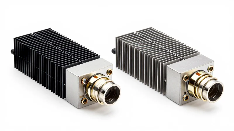
In the 400G landscape, the choice of form factor is a critical engineering decision that dictates the thermal efficiency, port density, and backward compatibility of data center switches. Silicon photonics plays a pivotal role here by enabling higher integration within these compact enclosures, directly addressing the power density challenges inherent in 400G transmissions.
QSFP-DD: Maximizing Density and Compatibility
The Quad Small Form-factor Pluggable Double Density (QSFP-DD) is the industry's most widely adopted 400G interface. Its primary advantage lies in its backward compatibility with legacy QSFP28 and QSFP+ modules. By adding a second row of electrical contacts, the QSFP-DD doubles the number of lanes from four to eight, supporting 8x50G PAM4 electrical modulation to achieve 400G throughput while maintaining the same front-panel density as previous generations.
OSFP: Superior Thermal Headroom for Next-Gen Scaling
The Octal Small Form-factor Pluggable (OSFP) is slightly wider and deeper than the QSFP-DD but offers significantly enhanced thermal management capabilities. Designed with an integrated heatsink, the OSFP can dissipate up to 15W or more, making it ideal for the early stages of 400G and 800G development where power consumption is often higher. While it requires an adapter for backward compatibility, its robust thermal design is a hedge against the heat generated by the high-speed DSPs required for long-reach optics.
| Feature | QSFP-DD | OSFP |
|---|---|---|
| Electrical Lanes | 8 Lanes (50G PAM4) | 8 Lanes (50G PAM4) |
| Backward Compatibility | Native (QSFP28/QSFP+) | Via Adapter Only |
| Max Power Consumption | Up to 12W - 14W | Up to 15W - 20W |
| Dimensions (Width) | 18.35 mm | 22.58 mm |
| Thermal Strategy | Rely on System Heatsink | Integrated Module Heatsink |
How Silicon Photonics Influences the Choice
Silicon Photonics (SiPh) is a game-changer for form factor selection because it typically consumes less power than discrete Indium Phosphide (InP) solutions. This lower power profile allows 400G SiPh transceivers to operate comfortably within the tighter thermal envelope of the QSFP-DD. By reducing the 'heat per bit,' SiPh enables operators to populate all 32 or 36 ports on a standard 1RU switch without hitting thermal throttling limits, a feat that is much more challenging with traditional laser technologies.
- Can QSFP-DD and OSFP interoperate?
Yes, they can interoperate at the optical level as long as they use the same wavelength and modulation (e.g., 400G-DR4). However, they are physically different and require specific cage designs on the switch hardware. - Which form factor is better for AI clusters?
OSFP is gaining significant traction in AI/ML clusters due to its higher power headroom, which is essential for the ultra-high-speed 800G and 1.6T transitions currently being fast-tracked. - Does SiPh make QSFP-DD more reliable?
Generally, yes. By integrating multiple optical components onto a single silicon chip, SiPh reduces the number of failure points and generates less waste heat, which is the primary driver of electronic degradation.
Key 400G Standards: DR4, FR4, and Beyond
Key 400G Standards: DR4, FR4, and Beyond
400G optical standards are primarily defined by the IEEE 802.3bs task force and various Multi-Source Agreements (MSAs) to ensure interoperability across different reach distances and fiber infrastructures. These standards utilize Pulse Amplitude Modulation (PAM4) at 53.125 GBaud to achieve 100G per lane, which Silicon Photonics (SiPh) platforms implement by integrating high-speed Mach-Zehnder modulators and multiplexing components on a single CMOS-compatible die. By standardizing the interface between the transceiver and the fiber plant, the industry allows for a mix-and-match approach to data center architecture, where SiPh provides the cost-and-power scaling necessary for high-volume deployment.
| Standard | Reach | Fiber Type | Wavelength Architecture | Modulation |
|---|---|---|---|---|
| 400G-DR4 | 500m | SMF (8-fiber) | 4 Parallel Lanes @ 1310nm | 100G PAM4 |
| 400G-DR4+ | 2km | SMF (8-fiber) | 4 Parallel Lanes @ 1310nm | 100G PAM4 |
| 400G-FR4 | 2km | SMF (2-fiber) | 4 Wavelengths CWDM4 | 100G PAM4 |
| 400G-LR4 | 10km | SMF (2-fiber) | 4 Wavelengths LWDM | 100G PAM4 |
400G-DR4: The Parallel Breakout Specialist
The DR4 standard is the most common deployment for intra-rack and inter-rack connections within hyperscale data centers. It utilizes four parallel lanes of single-mode fiber (SMF) for both transmission and reception. Silicon Photonics is uniquely suited for DR4 because it can integrate four separate modulators and four photodetectors on a single chip with high yields. The 'breakout' capability is a key advantage; a single 400G-DR4 port on a switch can be split into four 100G-DR interfaces, enabling high-density connectivity between top-of-rack switches and legacy 100G servers.
400G-FR4: Wavelength Efficiency via CWDM
The 400G-FR4 standard is designed for longer reaches up to 2km, optimized for switch-to-switch interconnects. Unlike DR4, which requires eight fibers (four Tx, four Rx), FR4 uses Coarse Wavelength Division Multiplexing (CWDM) to transmit four 100G signals over a single pair of fibers. Silicon Photonics simplifies FR4 module design by integrating the optical multiplexer and demultiplexer (typically an Echelle grating or Arrayed Waveguide Grating) directly into the silicon waveguide structure. This eliminates the need for complex, manual alignment of discrete thin-film filters, significantly lowering the cost of the optical engine.
Beyond 2km: LR4 and Future Coherent Standards
For campus and metropolitan distances reaching 10km and beyond, the 400G-LR4 standard employs LAN-WDM wavelengths to minimize chromatic dispersion. While traditional Indium Phosphide (InP) lasers have historically dominated this space, Silicon Photonics is making inroads through high-power integrated laser sources and advanced digital signal processing (DSP). Furthermore, for distances exceeding 40km, the industry is shifting toward coherent optics (400ZR/ZR+), where SiPh is the primary vehicle for integrating the complex IQ modulators and local oscillators required for coherent detection.
400G Connectivity Standards FAQ
- What is the main difference between DR4 and FR4?
The primary difference is the fiber requirement and wavelength usage. DR4 uses 8 fibers (parallel) at a single 1310nm wavelength, while FR4 uses only 2 fibers (duplex) by multiplexing 4 different wavelengths onto each fiber. - Does 400G Silicon Photonics support multi-mode fiber (MMF)?
Silicon Photonics is inherently a single-mode technology. For multi-mode fiber applications (such as 400G-SR8), VCSEL technology is typically used, as SiPh's waveguide dimensions are optimized for the narrow mode field of single-mode fiber. - Can a 400G-FR4 module talk to a 400G-DR4 module?
No. Because DR4 uses parallel fibers and FR4 uses wavelength division multiplexing on a single fiber, they are optically incompatible at the physical layer.
The Advantages of SiPh in Power Efficiency and Scalability
The Advantages of SiPh in Power Efficiency and Scalability
Silicon Photonics (SiPh) addresses the critical 'power wall' in modern data centers by integrating multiple optical components onto a single silicon substrate, thereby minimizing energy loss and maximizing production throughput via existing semiconductor infrastructures. By transitioning from discrete assembly to integrated circuits, 400G SiPh modules achieve the density and thermal efficiency required for next-generation hyperscale switching.
Driving Down Power-Per-Bit
In traditional 400G transceivers using discrete Indium Phosphide (InP) components, signal integrity often requires higher power to overcome parasitic capacitance and inductance at the interconnect level. Silicon Photonics reduces this overhead through high-density integration. By placing Mach-Zehnder Modulators (MZM) and waveguides in extremely close proximity to the CMOS drive electronics, the system minimizes transmission line losses and allows for lower voltage swings to achieve the same extinction ratios.
| Efficiency Metric | Traditional Discrete Optics | Silicon Photonics (SiPh) |
|---|---|---|
| Typical Power (Per 100G Lane) | ~2.5W - 3.5W | ~1.5W - 2.2W |
| Parasitic Loss | High (Wire bonding/Interconnects) | Low (Monolithic/Flip-chip) |
| Thermal Management | Complex (Hot spots from discrete lasers) | Efficient (Uniform heat distribution) |
Foundry-Scale Manufacturing and Yield
The primary economic advantage of SiPh is its compatibility with mature Complementary Metal-Oxide-Semiconductor (CMOS) fabrication processes. Unlike traditional optics that rely on specialized, smaller-scale InP foundries, SiPh transceivers are manufactured on standard 200mm or 300mm silicon wafers. This allows for thousands of photonic integrated circuits (PICs) to be produced in a single batch, utilizing the same lithography and automated inspection tools used for high-end microprocessors.
- How does SiPh improve manufacturing yields?
By employing automated wafer-level testing, manufacturers can identify defective photonic dies before they are ever packaged, significantly reducing the waste associated with final module assembly. - What is the impact on 400G deployment speed?
The ability to utilize existing semiconductor foundries means that as demand for 400G spikes, production can be ramped up far more quickly than traditional optics, which require labor-intensive manual alignment. - Does integration affect reliability?
Yes, positively. Reducing the number of discrete parts and fiber-to-chip couplings decreases the potential points of mechanical and thermal failure in the optical path.
Ultimately, the scalability of Silicon Photonics is what makes 400G—and the upcoming 800G and 1.6T standards—economically viable. As the industry moves toward co-packaged optics (CPO), the inherent power efficiency and foundry-friendly nature of silicon will become the standard requirement for all high-bandwidth interconnects.
Real-World Applications in High-Performance Computing (HPC)

The Role of 400G Silicon Photonics in HPC Architecture
In High-Performance Computing (HPC) environments, 400G Silicon Photonics (SiPh) serves as the critical interconnect fabric that allows thousands of processing nodes to function as a unified system. As workloads in AI training and scientific simulation grow, the bottleneck has shifted from raw compute power to the 'memory wall' and 'interconnect gap.' 400G SiPh addresses these challenges by providing massive throughput with ultra-low latency, enabling efficient East-West traffic flow between GPUs and CPUs across large-scale distributed clusters.
Distributed Computing and Interconnect Fabrics
Modern HPC clusters rely on parallel processing where sub-tasks are distributed across a vast array of nodes. 400G SiPh modules are integrated into InfiniBand and high-speed Ethernet fabrics to ensure that data synchronization between these nodes occurs at near-memory speeds. The integration of optical components onto a silicon substrate allows for higher port density and lower power consumption per bit, which is essential when managing the thermal envelopes of dense HPC racks containing high-wattage accelerators.
Storage Disaggregation and NVMe-over-Fabrics
Beyond compute, 400G SiPh is a primary driver for storage disaggregation. By using high-speed optical links, architects can decouple storage resources from compute nodes without sacrificing performance. This is achieved through protocols like NVMe-over-Fabrics (NVMe-oF), where 400G SiPh provides the high-capacity lanes needed to access remote flash storage with the same latency characteristics as local PCIe-attached drives.
| Feature | Passive Copper (DAC) | VCSEL (Multimode) | Silicon Photonics (Single Mode) |
|---|---|---|---|
| Max Distance | Up to 2.5m | Up to 100m | 2km to 10km+ |
| Power Efficiency | Highest | Moderate | High (Low per-bit) |
| Latency | Minimal | Low | Low |
| HPC Suitability | Intra-Rack only | Short-reach Cluster | Large-scale Distributed |
HPC Connectivity FAQs
- Why is Silicon Photonics preferred over traditional optics in HPC?
SiPh offers better scalability and reliability because it uses CMOS manufacturing processes to integrate multiple optical functions into a single chip, reducing component count and potential points of failure while lowering costs at high volumes. - Does 400G SiPh impact system-level latency?
No, 400G SiPh is designed for high-speed signal integrity. By reducing the need for heavy Forward Error Correction (FEC) in certain short-reach applications, it helps maintain the nanosecond-level latency required for HPC message passing. - Can 400G SiPh support future 800G or 1.6T upgrades?
Yes, the silicon photonics platform is inherently scalable. The same underlying technology used for 400G can be multiplexed or run at higher baud rates to reach 800G and 1.6T, providing a clear roadmap for HPC evolution.
Future Outlook: The Road to 800G and 1.6T

Future Outlook: The Road to 800G and 1.6T
The transition from 400G to 800G and eventually 1.6T represents more than just a speed increment; it is a fundamental shift in how optical interconnects are designed and integrated. While 400G Silicon Photonics (SiPh) has matured as a reliable solution for high-density data centers, the industry is now pivoting toward 800G and 1.6T solutions to satisfy the bandwidth-intensive requirements of Large Language Model (LLM) training and hyperscale AI clusters. Silicon Photonics is the primary engine of this growth, enabling the scalability and power efficiency required to reach terabit-level speeds.
The Technical Evolution Toward Terabit Ethernet
Scaling beyond 400G involves two primary technical levers: increasing the per-lane data rate and expanding the total number of lanes. The industry is currently moving from 112G SerDes toward 224G SerDes architectures. Silicon Photonics facilitates this by allowing for denser Photonic Integrated Circuits (PICs) that can manage higher-order modulation like PAM4 or even coherent detection in shorter reach applications, which were previously limited to long-haul networks.
| Generation | Aggregate Bandwidth | Per-Lane Rate | Key Technology Focus |
|---|---|---|---|
| 400G (Mature) | 400 Gbps | 50G/100G PAM4 | Pluggable QSFP-DD/OSFP |
| 800G (Emerging) | 800 Gbps | 100G/112G PAM4 | SiPh Integration & OSFP800 |
| 1.6T (Development) | 1600 Gbps | 200G/224G PAM4 | Co-Packaged Optics (CPO) |
Co-Packaged Optics (CPO): The Ultimate Integration
As speeds reach 1.6T, the physical distance between the switch ASIC and the optical transceiver becomes a critical bottleneck for power and signal integrity. Co-Packaged Optics (CPO) addresses this by moving the Silicon Photonics optical engine directly onto the same substrate as the ASIC. This proximity eliminates long electrical traces, drastically reducing power consumption per bit and minimizing latency. CPO is viewed as the inevitable end-state for data center networking, where Silicon Photonics' ability to be manufactured in CMOS-compatible foundries provides a significant cost and scale advantage.
- Why skip 800G and go straight to 1.6T in some labs?
Some hyperscalers are exploring 1.6T directly to maximize the efficiency of 51.2T and 102.4T switch ASICs, reducing the complexity of managing a larger number of lower-speed cables. - What is the biggest challenge for 1.6T Silicon Photonics?
Thermal management and the precision required for 224G SerDes signal integrity are the primary hurdles, requiring advanced cooling and new materials for optical modulators. - Will pluggable modules disappear entirely?
No. While CPO is the future for high-density cores, pluggable modules (OSFP/QSFP-DD) are expected to co-exist for several generations due to their ease of replacement and established maintenance workflows.
400G Silicon Photonics represents a paradigm shift in optical networking, offering the scalability and reliability required for the modern digital era. By leveraging silicon manufacturing, organizations can achieve high-speed data transmission with improved thermal and cost profiles. Ready to optimize your network infrastructure? Contact our engineering team for a technical consultation on 400G deployment.