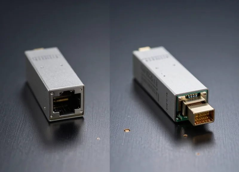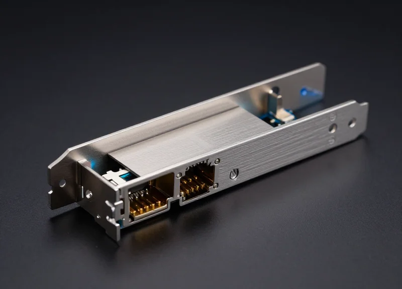
As Large Language Models (LLMs) and Generative AI applications grow exponentially, the underlying network infrastructure must evolve to handle massive data throughput. 800G optical transceivers have emerged as the critical link in AI clusters, offering the bandwidth, low latency, and density required to sustain modern GPU-to-GPU communication. This guide provides a veteran's perspective on the technical nuances of 800G optics and why they are the cornerstone of the AI era.
The Evolution of AI Fabrics: Why 800G Matters

The leap to 800G optical transceivers represents a fundamental response to the 'bandwidth wall' encountered in modern AI clusters. Unlike traditional cloud workloads, AI training relies on massive, synchronized data exchanges between thousands of GPUs, making the optical interconnect the primary determinant of total training time. As models grow in complexity, 800G serves as the vital link that prevents the network from becoming a bottleneck for high-performance compute nodes.
Architectural Shift: From General Purpose to AI-Specific Fabrics
Traditional data center architectures were primarily designed to handle 'North-South' traffic—data moving between the user and the server. In contrast, AI clusters are defined by 'East-West' traffic, where accelerators must constantly communicate to synchronize gradients and model weights. This shift necessitates a 'fat-tree' or non-blocking Clos topology where every bit of bandwidth must be utilized with minimal latency.
| Feature | Traditional Data Center | AI Training Cluster |
|---|---|---|
| Traffic Pattern | Predominantly North-South | Heavy East-West (GPU-to-GPU) |
| Latency Sensitivity | Moderate (Milliseconds) | Ultra-Low (Microseconds) |
| Standard Port Speed | 100G / 200G | 400G / 800G / 1.6T |
| Primary Objective | High Availability & Concurrency | Maximum Throughput & Synchronization |
The Impact of Distributed Training on Bandwidth
Large Language Models (LLMs) are now too massive to fit into the memory of a single GPU. Distributed training techniques, such as data and model parallelism, require collective communication operations like 'All-Reduce.' During these phases, the network must handle bursts of massive data transfers across the entire fabric. 800G optics, leveraging 112G SerDes technology, provide the necessary density and throughput to ensure that GPUs spend their time computing rather than waiting for data packets to arrive.
- Why is 800G preferred over 400G for new AI clusters?
800G provides higher radix for switches, allowing for flatter network topologies that reduce the number of hops and total system latency. - How does 800G affect power efficiency?
By moving more data per Watt through advanced DSPs and silicon photonics, 800G modules help keep the massive power demands of AI data centers under control. - What is the role of 112G SerDes in this evolution?
112G SerDes allows the optical module to match the native electrical signaling speed of the latest AI accelerators, eliminating the need for complex gearboxing.
800G Form Factors: OSFP vs. QSFP-DD800
800G Form Factors: OSFP vs. QSFP-DD800
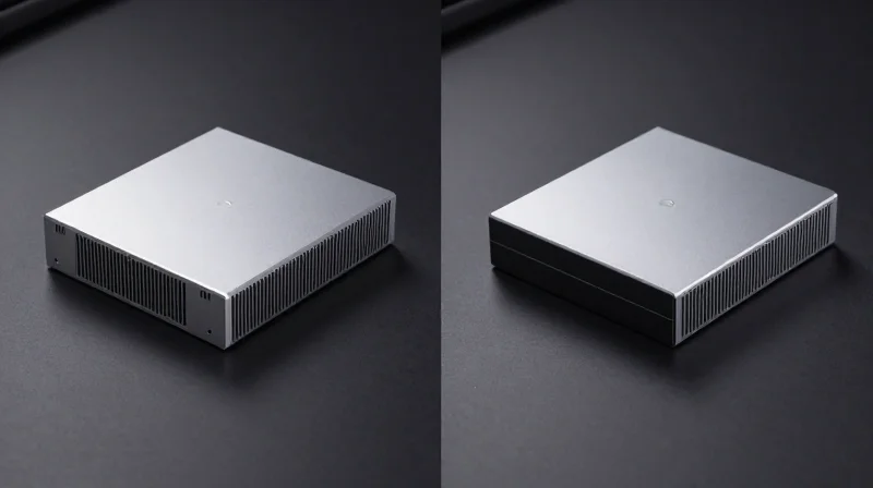
The choice between OSFP and QSFP-DD800 at the 800G tier is primarily a trade-off between thermal management and backward compatibility. While both form factors utilize 8 lanes of 112G SerDes to achieve 800G aggregate throughput, OSFP provides a superior thermal envelope essential for the high-power consumption of AI-grade DSPs, whereas QSFP-DD800 offers seamless mechanical integration with existing QSFP-based data center infrastructure.
OSFP: The Thermal Powerhouse for AI
The Octal Small Form-factor Pluggable (OSFP) was engineered to solve the cooling challenges of high-speed optics. By being slightly wider and deeper than legacy modules and incorporating an integrated heat sink, OSFP can dissipate power in excess of 15W to 20W. This headroom is critical for AI clusters where GPU-to-GPU communication via InfiniBand or high-radix Ethernet switches generates constant, heavy traffic loads that would otherwise lead to thermal throttling.
QSFP-DD800: Prioritizing Density and Legacy Support
QSFP-DD800 (Double Density) represents the evolution of the QSFP family, maintaining the same physical dimensions as the 400G QSFP-DD standard. Its primary advantage is native backward compatibility; a QSFP-DD800 port can accept 400G QSFP-DD, 100G QSFP28, or 40G QSFP+ modules without adapters. While this simplifies migration for traditional cloud data centers, the lack of an integrated heat sink makes cooling 800G components more difficult in the dense air-cooled racks common in AI training.
| Feature | OSFP | QSFP-DD800 |
|---|---|---|
| Thermal Capacity | Excellent (Integrated Heat Sink) | Moderate (External Heat Sink Required) |
| Backward Compatibility | Requires Mechanical Adapters | Native (QSFP-DD/QSFP28/QSFP+) |
| Dimensions (W x L) | 22.58mm x 107.8mm | 18.35mm x 89.4mm |
| Typical AI Use Case | NVIDIA InfiniBand & High-Performance Fabrics | Hyperscale Ethernet Aggregation |
Form Factor Selection FAQ
- Why is OSFP dominant in NVIDIA-based AI clusters?
NVIDIA's networking stacks, including Quantum-2 InfiniBand and Spectrum-4 Ethernet, utilize OSFP because its superior thermal characteristics support the high-power requirements of the transceivers and active optical cables (AOCs) needed for massive-scale GPU synchronization. - Can QSFP-DD800 be used for 800G AI applications?
Yes, QSFP-DD800 is widely used in AI clusters that leverage standardized Ethernet switches. However, it requires more robust system-level cooling solutions (such as liquid cooling or high-CFM fans) to manage the heat generated by 800G DSPs within the smaller module volume. - Does OSFP impact port density compared to QSFP-DD?
While OSFP is wider, modern switch designs allow for 32 to 36 ports of either form factor in a standard 1U chassis, meaning there is no significant sacrifice in port density when choosing the more thermally efficient OSFP.
Modulation and Electrical Interface: 112G SerDes and PAM4
The Architecture of Throughput: 8x112G SerDes
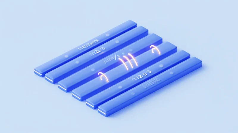
800G optical transceivers achieve their massive throughput by utilizing an electrical interface consisting of eight parallel lanes, each operating at 112.5 Gbps. This 112G SerDes (Serializer/Deserializer) technology is the critical link between the Switch ASIC and the optical engine, doubling the lane density from the previous 56G generation. By maintaining an 8-lane configuration, 800G modules can fit within established form factors like OSFP and QSFP-DD800 while providing the bandwidth required for low-latency collective communication in AI training clusters.
PAM4: The Modulation Engine of 800G
To achieve 112Gbps per lane without requiring exorbitant electrical bandwidth that would lead to signal degradation, 800G systems employ 4-level Pulse Amplitude Modulation (PAM4). Unlike traditional Non-Return-to-Zero (NRZ) which transmits one bit per symbol, PAM4 transmits two bits per symbol by using four distinct voltage levels. This approach effectively halves the required Nyquist frequency for a given bit rate, allowing 112G data to travel across PCB traces and connectors that would otherwise be unable to support the frequency demands of NRZ at such speeds.
| Feature | NRZ (1x56G) | PAM4 (1x112G) |
|---|---|---|
| Bits per Symbol | 1 bit | 2 bits |
| Signal Levels | 2 (0, 1) | 4 (00, 01, 10, 11) |
| Symbol Rate (Baud) | 56 GBaud | 56 GBaud |
| SNR Penalty | 0 dB (Reference) | ~9.5 dB |
| Primary Application | 400G and below | 800G / 1.6T |
Signal Integrity and the Role of DSP
The transition to PAM4 introduces a significant signal-to-noise ratio (SNR) challenge, as the compressed voltage levels are more susceptible to noise and interference. To mitigate this, 800G transceivers incorporate high-performance Digital Signal Processors (DSP). The DSP performs complex equalization (such as FFE and DFE) and works in tandem with Forward Error Correction (FEC) algorithms, specifically KP4 FEC defined in IEEE 802.3ck. These technologies ensure that even with the inherent noise sensitivity of 112G PAM4, the system maintains a bit error rate (BER) low enough for the lossless transmission required by InfiniBand and Ethernet AI fabrics.
- Why is 112G per lane the industry standard for 800G?
It allows 800G throughput to be delivered via 8 lanes, matching the electrical pin-out capacity of high-density form factors like OSFP while aligning with the evolution of 51.2T Switch ASICs. - What is the primary trade-off of using PAM4?
The primary trade-off is increased complexity and power consumption; the DSP required to decode 4-level signals consumes significantly more energy than simple NRZ drivers. - How does 112G SerDes affect PCB design?
It mandates the use of ultra-low-loss PCB materials and precision-engineered connectors to minimize insertion loss and crosstalk at the 28GHz Nyquist frequency.
Key Variants: 800G SR8, DR8, and 2xFR4 Explained
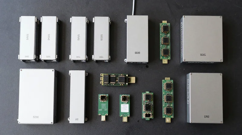
The diversity in 800G optical transceiver standards is driven by the need to optimize for cost, power consumption, and physical reach across the three-tier Clos architectures used in AI clusters. While the electrical interface remains a standardized 8x112G PAM4, the optical interface varies significantly: SR8 leverages low-cost multimode fiber for rack-scale links, DR8 provides parallel single-mode capacity for low-latency spine connections, and 2xFR4 employs wavelength division multiplexing (WDM) to maximize fiber efficiency over longer distances.
800G SR8: Cost-Effective Short-Reach Connectivity
The 800G SR8 variant is designed for 'Short Reach' applications, typically limited to 60 to 100 meters over OM4 multimode fiber (MMF). It utilizes eight channels of 100G PAM4, each powered by a Vertical-Cavity Surface-Emitting Laser (VCSEL). Because VCSELs and multimode fibers are significantly cheaper than their single-mode counterparts, SR8 is the primary choice for connecting AI accelerators (like GPUs) to Top-of-Rack (ToR) switches within the same or adjacent racks.
800G DR8: Parallel Single-Mode for AI Spines
The 800G DR8 (Data center Reach) variant extends the reach to 500 meters using single-mode fiber (SMF). Unlike SR8, it uses Silicon Photonics (SiPh) or Externally Modulated Lasers (EML). It employs a parallel design with 8 fibers for Tx and 8 for Rx (typically via an MPO-16 connector). DR8 is critical for AI clusters where the physical distance between the leaf and spine switches exceeds the limits of multimode fiber, offering a balance of high bandwidth and low-latency signal propagation.
800G 2xFR4: Maximizing Fiber Efficiency via WDM
The 2xFR4 variant represents a more complex architecture that aggregates two 400G FR4 links into a single 800G module. It uses Coarse Wavelength Division Multiplexing (CWDM) to transmit four wavelengths (1271, 1291, 1311, and 1331nm) over a single pair of fibers. By reducing the fiber count from 16 (in DR8) to just 4 fibers per 800G link, 2xFR4 is the preferred solution for 2km reaches where fiber duct space is at a premium or cabling costs are prohibitive.
Comparative Analysis of 800G Optical Variants
| Feature | 800G SR8 | 800G DR8 | 800G 2xFR4 |
|---|---|---|---|
| Fiber Type | Multimode (OM3/OM4) | Single-mode (SMF) | Single-mode (SMF) |
| Max Reach | 60m (OM3) / 100m (OM4) | 500m | 2km |
| Light Source | 850nm VCSEL | 1310nm SiPh/EML | CWDM4 EML |
| Connector | MPO-16 / MPO-12 | MPO-16 / MPO-12 | Dual CS / Dual LC |
| Primary Use Case | GPU to ToR Switch | Leaf to Spine Switch | Inter-building / Aggregation |
Common Implementation Questions
- Can 800G DR8 be used for breakout applications?
Yes, DR8 is highly versatile for breakouts. It can be split into two 400G DR4 links or eight 100G DR1 links, which is essential for connecting high-radix 800G switches to legacy 100G or 400G endpoints. - Why is 2xFR4 gaining popularity in AI back-end networks?
As AI clusters scale to thousands of nodes, fiber management becomes a nightmare. 2xFR4 reduces the required fiber cabling by 75% compared to DR8 while supporting the 2km distances often required in mega-data center campuses. - Which variant is most sensitive to power consumption?
SR8 typically has the lowest power consumption (~12-14W) due to the efficiency of VCSELs, whereas 2xFR4 can reach 16-18W because of the internal multiplexers and cooling requirements for EML lasers.
Addressing Power Constraints: LPO and LRO Technologies
As AI workloads scale, the thermal density of 800G transceivers becomes a bottleneck, with traditional DSP-based modules consuming significant power and introducing nanosecond-level latency. Linear Drive Pluggable Optics (LPO) and Linear Receive Optics (LRO) address these constraints by leveraging the host switch's high-performance SerDes for signal equalization, effectively eliminating or reducing the need for power-hungry processing within the optical module itself.
Linear Drive Pluggable Optics (LPO): Maximum Efficiency
LPO is a 'DSP-free' architecture where the optical transceiver contains only high-linearity drivers and Transimpedance Amplifiers (TIAs). By removing the DSP, LPO modules can reduce power consumption by approximately 50% compared to standard 800G modules. This reduction is critical for high-density AI racks where cooling capacity is limited. Furthermore, LPO reduces latency to the picosecond range because there is no digital-to-analog conversion or complex signal processing, which is a major advantage for synchronized GPU-to-GPU communication.
Linear Receive Optics (LRO): The Hybrid Compromise
While LPO offers the lowest power, it places a heavy burden on the host ASIC's SerDes to handle signal integrity for both transmit and receive paths. Linear Receive Optics (LRO) provides a middle ground. In an LRO configuration, the transmit side of the module retains a simplified DSP or retimer to ensure signal quality to the fiber, while the receive side remains linear (DSP-less). This hybrid approach offers better interoperability and reach than LPO while still achieving significant power savings over full-DSP modules.
Technical Comparison: DSP-Based vs. LPO vs. LRO
| Feature | Standard DSP-Based 800G | 800G LPO | 800G LRO |
|---|---|---|---|
| Power Consumption | 14W - 18W | ~8W - 10W | ~10W - 12W |
| Latency | ~100ns (DSP processing) | < 1ns | ~50ns (Tx side only) |
| Interoperability | High (Plug and Play) | Low (Requires host tuning) | Medium |
| Primary Use Case | General Data Center / Long Reach | High-Density AI / GPU Clusters | Optimized AI Networking |
Design Challenges in Linear Architectures
The primary challenge for LPO and LRO is signal integrity. Without a DSP to 'clean up' the signal within the module, the host switch or NIC must have a robust SerDes capable of compensating for the entire link's impairments. This necessitates a tighter integration between the optical module vendor and the switch silicon provider. Furthermore, LPO is generally restricted to shorter reaches (typically under 100 meters) because the signal degradation over long fiber spans requires the sophisticated error correction and equalization that only a full DSP can provide.
FAQ: LPO and LRO in 800G AI Networks
- Why is LPO becoming popular for AI clusters specifically?
AI clusters require massive bandwidth with minimal latency. LPO eliminates the DSP latency and significantly lowers the heat generated in the rack, allowing for higher port density. - Can I use LPO modules with any 800G switch?
No, LPO requires the host switch's SerDes to support linear drive characteristics. It is not a universal plug-and-play solution like standard DSP modules. - Does LRO support longer distances than LPO?
Generally, yes. Because LRO maintains a DSP on the transmit path, it can better maintain signal quality over the fiber, making it more robust for varied link lengths within a data center.
The Impact of Silicon Photonics on 800G Production
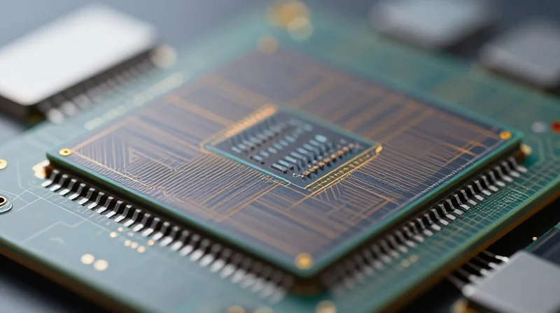
Silicon Photonics (SiPh) is the primary catalyst for the mass adoption of 800G optical transceivers, shifting the industry from labor-intensive discrete component assembly to automated, wafer-level semiconductor manufacturing. By integrating lasers, modulators, and detectors onto a single silicon substrate, SiPh significantly lowers the bill of materials (BOM) and enhances the thermal stability required for the high-density environments of AI data centers.
The Transition from Discrete Optics to Integrated Silicon Photonics
Traditional optical manufacturing relies on 'Gold-box' packaging, where individual components like Indium Phosphide (InP) lasers and modulators are manually or semi-automatically aligned. At 800G speeds, the precision required for these alignments becomes a bottleneck for yield and cost. Silicon Photonics solves this by using mature CMOS fabrication processes to etch optical circuits directly into silicon wafers. This allows for thousands of transceivers to be tested at the wafer level before they are even diced, drastically improving production throughput.
| Feature | Traditional Discrete Optics | Silicon Photonics (SiPh) |
|---|---|---|
| Manufacturing | Manual/Discrete Assembly | Automated Wafer-Level CMOS |
| Integration | Low (Multiple chips/packages) | High (Monolithic/Hybrid integration) |
| Reliability | Variable (High part count) | High (Simplified signal paths) |
| Cost Scalability | Linear (Cost grows with volume) | Exponential (Cost drops with volume) |
| Typical 800G Reach | FR4 / LR4 (Longer distances) | DR8 / DR4+ (Short to Medium reach) |
Emerging Tech: Thin-Film Lithium Niobate (TFLN)
While SiPh is the workhorse for current 800G DR8 deployments, Thin-Film Lithium Niobate (TFLN) is emerging as a critical material for high-performance modulators. TFLN combines the high-speed modulation capabilities of traditional Lithium Niobate with the small form factor of thin-film technology. For AI clusters, this means 800G modules can operate with lower drive voltages and higher bandwidth, directly addressing the power efficiency concerns inherent in massive GPU fabrics.
Production Scaling and Reliability FAQ
- Does Silicon Photonics improve the reliability of 800G links?
Yes. By reducing the number of physical interconnects and fiber-to-chip couplings within the module, SiPh minimizes potential points of failure, which is vital when managing thousands of links in a single AI cluster. - How does TFLN compare to Silicon Photonics for 800G?
TFLN offers superior linearity and lower insertion loss than standard SiPh modulators. While SiPh is currently more cost-effective for 500m reaches (DR8), TFLN is increasingly preferred for 2km+ reaches (FR4) and future 1.6T transitions due to its bandwidth headroom. - What is the impact of SiPh on 800G lead times?
Because SiPh leverages existing semiconductor foundries, production can be scaled much faster than traditional optical components, leading to more stable supply chains for hyper-scale data centers.
Network Protocol Synergy: InfiniBand vs. RoCE v2
The Intersection of 800G Hardware and Transport Protocols
The performance of 800G optical transceivers in AI clusters is not merely a function of raw bandwidth but is deeply tied to the underlying network protocol. Whether deploying InfiniBand or RDMA over Converged Ethernet (RoCE v2), the 800G physical layer must support high-throughput, low-latency data transfers to prevent GPU 'starvation.' InfiniBand provides a lossless, credit-based environment optimized for short-packet AI traffic, while RoCE v2 leverages the ubiquity of Ethernet with specialized congestion control mechanisms to achieve similar efficiencies at a different scale.
InfiniBand: Native Lossless Performance at 800G
In the context of 800G, InfiniBand (specifically NDR and future XDR generations) utilized OSFP and QSFP-DD transceivers to maintain a strictly lossless fabric. Because AI training involves massive, synchronized 'All-Reduce' operations, any packet loss leads to significant retransmission delays. InfiniBand's hardware-level flow control ensures that 800G links are saturated with minimal overhead, making it the preferred choice for massive-scale GPU clusters where sub-microsecond latency is non-negotiable.
RoCE v2: Leveraging 800G Ethernet Ubiquity
RoCE v2 enables Remote Direct Memory Access (RDMA) over standard Ethernet frames, allowing 800G transceivers to integrate into existing data center switching architectures. To compete with InfiniBand, RoCE v2 relies on Priority Flow Control (PFC) and Data Center Quantized Congestion Notification (DCQCN). For 800G deployments, this means the transceivers must interface with advanced Ethernet switches capable of managing high-density traffic without dropping packets, balancing the cost-effectiveness of Ethernet with the performance demands of Large Language Models (LLMs).
| Feature | InfiniBand (NDR/XDR) | RoCE v2 (800G Ethernet) |
|---|---|---|
| Flow Control | Credit-based (Hardware level) | PFC / ECN (Software/Hardware hybrid) |
| Latency | Ultra-low, deterministic | Low, but varies with congestion |
| Scalability | Specialized, high-density pods | Massive, standard DC fabrics |
| Transceiver Type | Optimized OSFP (NVIDIA spec) | Standard OSFP/QSFP-DD |
| Management | Subnet Manager (Centralized) | Standard SDN / SNMP (Decentralized) |
Protocol Selection FAQ
- Can 800G transceivers be interchanged between InfiniBand and RoCE networks?
While the physical form factors (OSFP/QSFP-DD) are often identical, the firmware and optical specifications may differ. NVIDIA-specific InfiniBand optics are often required for InfiniBand switches, whereas RoCE v2 typically uses standard-compliant Ethernet transceivers. - Does 800G RoCE v2 perform as well as 800G InfiniBand for AI?
For most mid-sized clusters, the performance is comparable. However, at the extreme scale of tens of thousands of GPUs, InfiniBand's native lossless architecture often provides a slight edge in tail latency and job completion time. - How does 800G optics affect power consumption in these protocols?
The protocol itself has a negligible impact on the transceiver's power draw; however, the efficiency of the protocol dictates how long the transceiver must remain in a high-power state to complete a data transfer.
Deployment Challenges: Thermal Management and Signal Integrity

Navigating the Constraints of 800G: Heat and Signal Fidelity
Deploying 800G optical transceivers in AI clusters introduces a non-linear increase in technical difficulty compared to 400G generations. The primary challenges stem from a doubling of data rates per lane—moving to 112G or 224G SerDes—which drastically reduces signal margins, and the concentrated power density of modules that can now exceed 16 to 18 watts each. Failure to manage these factors leads to increased Bit Error Rates (BER) and thermal throttling, which can cripple the low-latency requirements of large-scale AI training jobs.
The Thermal Bottleneck: Managing High-Density Power Dissipation
As 800G OSFP and QSFP-DD modules reach power consumption levels of 15W-18W, traditional air-cooling methods reach their physical limits. In a 1U switch with 32 ports, the total heat generated by optics alone can exceed 500W. This necessitates advanced heat sink designs with higher fin density and, increasingly, a shift toward liquid cooling or 'cool-plug' technologies. Thermal management is not just about preventing hardware failure; it is about maintaining laser stability, as temperature fluctuations cause wavelength shifts that degrade optical performance.
| Metric | 400G (QSFP-DD) | 800G (OSFP/QSFP-DD800) |
|---|---|---|
| Typical Power Consumption | 10W - 12W | 14W - 18W |
| SerDes Speed per Lane | 56G / 112G PAM4 | 112G / 224G PAM4 |
| Max Reach (Copper DAC) | Up to 3 meters | Less than 2 meters |
| Thermal Management | Standard Airflow | High-Airflow / Liquid Cooling |
Signal Integrity and the 112G SerDes Barrier
At 112G per lane, the electrical channel between the switch ASIC and the optical module suffers from severe insertion loss. The 'reach' of traditional passive copper cables (DACs) has shrunk significantly, often to less than 2 meters, making them impractical for many AI rack architectures. To counter this, 800G systems rely heavily on sophisticated Digital Signal Processors (DSP) within the module to perform equalization and error correction. However, these DSPs are themselves the primary contributors to the heat problems mentioned above, creating a design paradox that engineers must balance through power-efficient CMOS processes.
- Why is signal integrity harder at 800G than 400G?
Higher frequencies lead to greater attenuation and crosstalk on the PCB. The transition to 112G lanes reduces the unit interval (UI), making the system much more sensitive to jitter and noise. - Can liquid cooling solve the 800G thermal issue?
Yes, immersion cooling and cold-plate technologies are being adopted in AI data centers to efficiently remove heat from high-density 800G switch ports where air cooling is insufficient. - What is the role of FEC in 800G signal integrity?
Forward Error Correction (FEC) is essential at 800G to resolve errors caused by signal degradation, though it adds a small amount of latency to the network path.
The Roadmap to 1.6T: Preparing for the Next Leap
The Roadmap to 1.6T: Preparing for the Next Leap
800G optical transceivers are not merely an incremental upgrade; they serve as the foundational architecture for the eventual deployment of 1.6T interconnects. By establishing the power density and thermal management protocols required for 112G-per-lane signaling, the industry is now paving the way for 224G SerDes (Serializer/Deserializer) technology. This transition will double the throughput per port while maintaining the same physical footprint, effectively addressing the bandwidth-per-rack density requirements of future Large Language Model (LLM) training cycles.
The Shift to 224G SerDes and Signal Integrity
The jump to 1.6T is fundamentally tied to the evolution of SerDes speed. While current 800G modules utilize 8 lanes of 112G (PAM4), 1.6T transceivers will leverage 8 lanes of 224G. This leap presents significant challenges in signal integrity, requiring advanced DSPs with lower latency and higher jitter tolerance. Linear Drive Optics (LDO) and Co-Packaged Optics (CPO) are emerging as critical pathways to reduce power consumption by removing or minimizing the reliance on energy-intensive DSP chips directly within the module.
| Feature | 800G Transceiver (Current) | 1.6T Transceiver (Future) |
|---|---|---|
| Electrical Interface | 8x112G SerDes | 8x224G SerDes |
| Modulation | PAM4 | PAM4 / PAM6 / Coherent |
| Form Factors | OSFP, QSFP-DD | OSFP1600, QSFP-DD1600 |
| Power Target | 16W - 24W | 25W - 35W |
| Primary Use Case | H100/H200 Clusters | Next-Gen AI Accelerators (Blackwell+) |
Form Factor Evolution: OSFP1600 and Beyond
To accommodate the thermal demands of 1.6T, the OSFP (Octal Small Form-factor Pluggable) design is evolving into the OSFP1600. This version maintains backward compatibility but enhances cooling fins and connector pin density to handle higher currents and heat dissipation. The goal is to allow data centers to transition from 800G to 1.6T without a complete overhaul of the cooling infrastructure, though liquid cooling at the switch level is increasingly becoming a prerequisite for 1.6T density.
- When will 1.6T transceivers be commercially available?
Initial sampling of 1.6T modules has begun in 2026, with large-scale commercial deployment expected in late 2025 and 2026, coinciding with the next generation of AI switch silicon. - Can 800G infrastructure support 1.6T?
While fiber plants (SMF/MMF) remain largely compatible, the active components—switches and network interface cards (NICs)—must be upgraded to support 224G SerDes signaling. - Will 1.6T use Silicon Photonics?
Yes, Silicon Photonics (SiPh) and Thin-Film Lithium Niobate (TFLN) are expected to be the dominant technologies for 1.6T to manage the tighter power budgets and higher modulation speeds.
800G optical transceivers are no longer a luxury but a necessity for any enterprise or cloud provider scaling AI workloads. By understanding the nuances of form factors, modulation, and power efficiency, network architects can build future-proof AI fabrics that eliminate data bottlenecks. Ready to optimize your cluster? Contact our technical team today for a custom 800G connectivity roadmap.