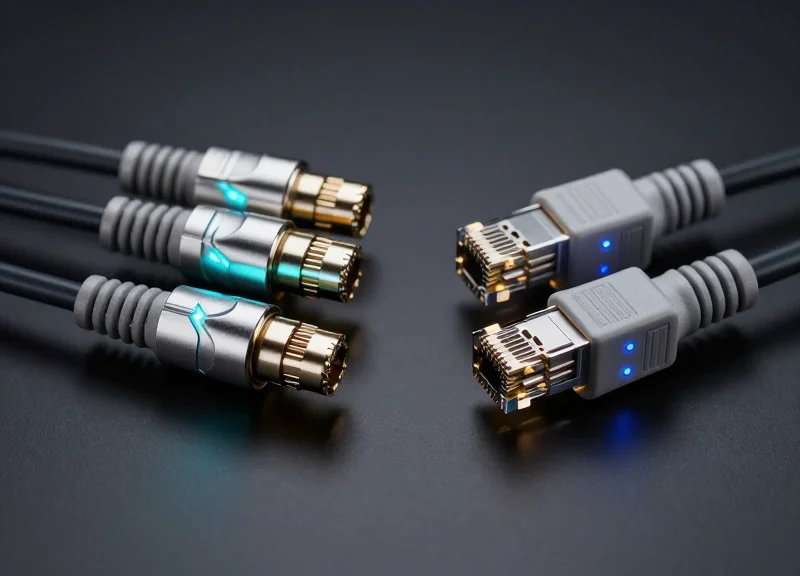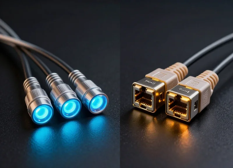
The explosion of generative AI and large language models has pushed data center traffic to its breaking point. As 800G reaches maturity, the industry is pivoting toward 1.6T Evolution to double throughput and maintain the pace of innovation. This article explores the technical foundations, hardware breakthroughs, and strategic importance of this massive leap in optical networking.
The Roadmap to 1.6T: Driving Forces Behind the Shift

The AI Catalyst: Why 800G is Reaching Its Limits
The evolution to 1.6T is primarily driven by the 'AI arms race,' where the scale of Large Language Models (LLMs) requires massive GPU clusters to communicate with near-zero latency and unprecedented throughput. While 800G was a significant milestone, it is becoming a bottleneck for the latest generation of AI accelerators that demand higher 'East-West' traffic capacity to synchronize trillions of parameters across distributed nodes.
Comparative Analysis: 800G vs. 1.6T Infrastructure
| Metric | 800G Standard | 1.6T Evolution |
|---|---|---|
| Throughput per Port | 800 Gbps | 1.6 Tbps |
| SerDes Lane Rate | 112G (PAM4) | 224G (PAM4) |
| Standard Lane Count | 8 x 100G | 8 x 200G or 16 x 100G |
| Primary Use Case | Hyperscale Cloud | Generative AI Training Clusters |
Driving Forces Behind the 1.6T Shift
The shift is not just about raw speed; it is about efficiency and density. The move to 1.6T enables data centers to maintain the same physical footprint while doubling their capacity. This is achieved by transitioning from 112G SerDes to 224G SerDes technology, which allows for 1.6T throughput using an 8-lane configuration. Reducing the number of physical links and switches required to move a specific volume of data directly translates to lower power consumption per bit—a critical metric for modern sustainable computing.
Frequently Asked Questions About 1.6T Roadmap
- What is the main technical hurdle for 1.6T?
The primary challenge lies in signal integrity at 224G SerDes speeds. As frequencies increase, signal loss and electromagnetic interference become more pronounced, requiring advanced PCB materials and more sophisticated Digital Signal Processing (DSP). - How does 1.6T impact AI training times?
By doubling the bandwidth between compute nodes, 1.6T significantly reduces the communication overhead during the 'All-Reduce' phase of AI training, allowing GPUs to spend more time computing and less time waiting for data transfer. - Will 1.6T replace 800G immediately?
No. 1.6T will initially coexist with 800G, serving as the high-speed backbone for top-tier AI clusters, while 800G remains the standard for general-purpose cloud computing for the next several years.
Furthermore, the roadmap to 1.6T is heavily influenced by the emergence of Co-Packaged Optics (CPO) and Linear Drive Pluggable Optics (LPO). These technologies aim to move the optical engine closer to the switch silicon, further reducing power loss and enabling the high-density radix configurations necessary for the next generation of 51.2T and 102.4T switching silicon.
Defining the Standard: The Role of IEEE 802.3dj
The IEEE 802.3dj Task Force represents the most ambitious expansion of the Ethernet standard to date, specifically targeting the development of physical layer (PHY) specifications that support aggregate speeds of 800 Gb/s and 1.6 Tb/s. By doubling the per-lane throughput from the previous 100 Gbps (802.3ck) standard to 200 Gbps, the 802.3dj project addresses the immediate bandwidth bottlenecks inherent in hyperscale data centers and the massive I/O requirements of AI backend fabrics.
The Core Objectives of IEEE 802.3dj
The scope of 802.3dj extends beyond mere speed increases; it is designed to provide a comprehensive ecosystem for various interconnect lengths and media types. The task force is standardizing the signaling necessary to transport data over copper, backplanes, and fiber optics, ensuring that 1.6T can be deployed across the entire data center hierarchy.
| Feature | IEEE 802.3ck (800G Era) | IEEE 802.3dj (1.6T Era) |
|---|---|---|
| Max Lane Rate | 100 Gbps per lane | 200 Gbps per lane |
| Aggregate Speed | Up to 800 Gbps | Up to 1.6 Terabits per second |
| Primary Modulation | PAM4 | Advanced PAM4 / Higher Order |
| Target Media | CU, Backplane, MMF, SMF | CU, Backplane, SMF (Up to 10km) |
| Main Application | Cloud Infrastructure | AI/ML Training Clusters |
Technical Challenges: Signal Integrity at 200G
The move to 200 Gbps per lane introduces significant physical challenges. At these frequencies, signal attenuation and insertion loss in copper traces and cables become much more pronounced. To combat this, IEEE 802.3dj is exploring sophisticated Forward Error Correction (FEC) architectures. These new FEC schemes must balance the need for low latency—critical for AI training—with the robust error correction required for high-speed signaling across varied physical distances.
Standardization FAQ
- Why is 200G per lane necessary for 1.6T?
Scaling to 1.6T using 100G lanes would require 16 parallel lanes, resulting in bulky connectors and high power consumption. 200G per lane allows for 8-lane configurations, maintaining the 8-lane density standard common in OSFP and QSFP-DD form factors. - Does 802.3dj support backwards compatibility?
Yes, the standard is designed to ensure that 1.6T ports can negotiate down to 800G or 400G, protecting existing infrastructure investments while providing a clear upgrade path. - What is the timeline for adoption?
While the 802.3dj standard is still being refined by the IEEE, early silicon and physical layer prototypes are already appearing in the market, with mass adoption expected following the final ratification around 2026.
224G SerDes: The Heart of 1.6T Connectivity

At the core of the 1.6T evolution lies the 224G SerDes (Serializer/Deserializer), the critical physical layer component that enables the transmission of 224 Gbps per electrical lane. By doubling the per-lane throughput from the previous 112G standard, 224G SerDes allows for the 8-lane configurations necessary to reach 1.6 Tbps aggregate bandwidth while maintaining manageable form factors and power envelopes in next-generation data centers.
Signal Integrity: Navigating the 56 GHz Nyquist Frontier
Scaling to 224G introduces profound signal integrity challenges, primarily because the Nyquist frequency doubles to approximately 56 GHz. At these extreme frequencies, physical traces on PCBs act as antennas, and dielectric loss becomes a dominant factor. Engineers must contend with significantly higher insertion loss, increased crosstalk, and tighter jitter budgets that leave almost no room for error in channel design.
| Parameter | 112G SerDes | 224G SerDes |
|---|---|---|
| Nyquist Frequency | 28 GHz | 56 GHz |
| Baud Rate | 53.125 GBd | 106.25 GBd |
| Reach Capacity | ~1-2 meters (DAC) | < 1 meter (DAC) / Linear Drive |
| Typical Modulation | PAM4 | PAM4 (Enhanced) |
The Evolution of PAM4 and DSP Requirements
While 224G continues to utilize PAM4 (Pulse Amplitude Modulation 4-level) signaling, the signal-to-noise ratio (SNR) requirements are far more stringent than in previous generations. To compensate for the 30-40dB of channel loss expected at 224G, hardware designers are leaning heavily on advanced Digital Signal Processing (DSP). These chips now incorporate more complex equalization algorithms, such as Maximum Likelihood Sequence Estimation (MLSE) and more robust Forward Error Correction (FEC) schemes, to recover signals from the noise floor.
The Shift to Linear Drive and CPO
Because traditional retimed modules consume significant power at 224G, the industry is evaluating Linear Drive Pluggable Optics (LPO) and Co-Packaged Optics (CPO). These architectures reduce the electrical path length between the SerDes and the optical engine, effectively bypassing some of the signal integrity hurdles inherent in long PCB traces and complex connectors.
- Why can't we just use PAM8 for 224G?
While PAM8 provides more bits per symbol, the reduction in signal-to-noise ratio (SNR) margin makes it technically prohibitive for 224G electrical lanes compared to the more mature and robust PAM4 modulation. - What is the primary bottleneck for 224G adoption?
The primary bottleneck is the 'Reach'—the physical distance a signal can travel before becoming unreadable. This necessitates shorter copper cables or a faster transition to optical interconnects. - How does 224G impact PCB material choice?
It requires ultra-low-loss dielectric materials and smoother copper foils to minimize skin-effect losses and signal attenuation at 56 GHz.
Optical Form Factors: The Rise of OSFP-XD
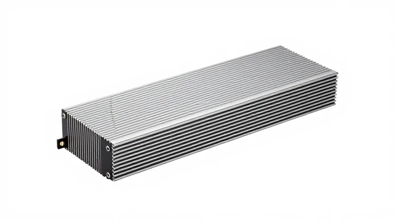
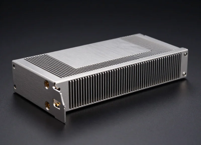
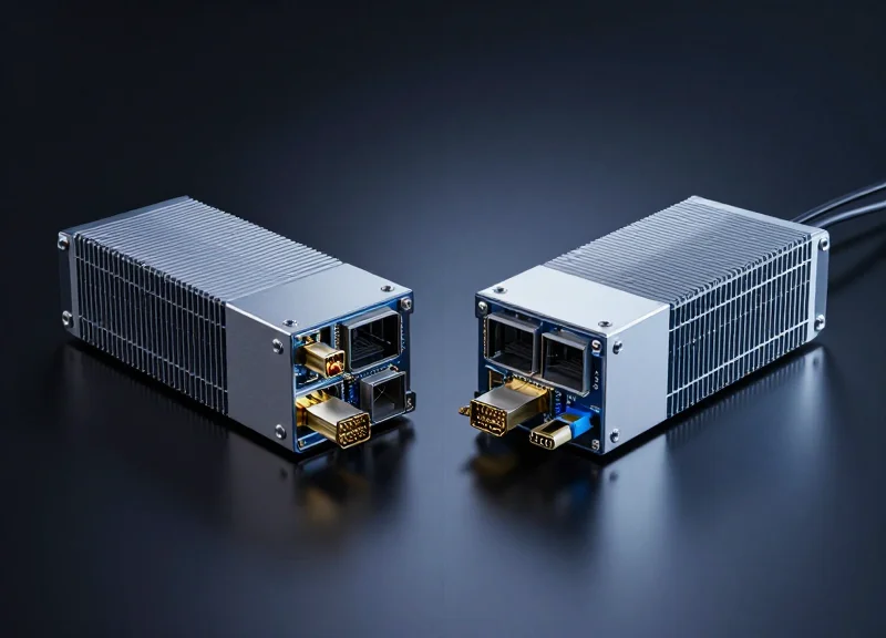
The transition to 1.6T connectivity requires more than just faster SerDes; it demands a physical housing capable of managing double the data throughput within a standard 1RU switch faceplate. The OSFP-XD (Extra Density) form factor addresses this by doubling the electrical connector pin count to support 16 lanes. This allows for 1.6T throughput using existing 100G-per-lane technology in the short term, while providing the thermal headroom necessary for 200G-per-lane optics as 1.6T moves into mass deployment.
Comparative Analysis: OSFP vs. OSFP-XD
| Feature | Standard OSFP | OSFP-XD |
|---|---|---|
| Electrical Lanes | 8 Lanes | 16 Lanes |
| Max Bandwidth (100G SerDes) | 800 Gbps | 1.6 Tbps |
| Max Bandwidth (200G SerDes) | 1.6 Tbps | 3.2 Tbps |
| Power Consumption Capacity | 15W - 20W | 30W - 40W |
| Connector Density | Standard | Double (Stacked/XD) |
Thermal Management: The 30W Challenge
Heat dissipation is the primary barrier to 1.6T scaling. As transceiver power consumption climbs toward 30 watts per module, the ability to pull heat away from the DSP and optical engine becomes paramount. OSFP-XD leverages an integrated heat sink and an optimized airflow path that utilizes the larger surface area of the OSFP footprint. This design allows for a 1.6T switch to maintain a 51.2T or 102.4T total capacity without reaching thermal throttling, a feat that is significantly more difficult to achieve with the smaller thermal window of the QSFP-DD form factor.
Density and Faceplate Efficiency
By utilizing 16 electrical lanes, OSFP-XD enables hardware manufacturers to maintain the same port count on a switch faceplate while doubling the capacity per port. This density is essential for AI clusters where thousands of GPUs must be interconnected with minimal latency and physical footprint. The OSFP-XD cage is also designed for backward compatibility, ensuring that standard 8-lane OSFP modules can still be utilized in XD ports, providing a flexible migration path for data center operators.
Common Questions Regarding OSFP-XD
- Is OSFP-XD backward compatible with standard OSFP?
Yes, OSFP-XD cages are designed to be backward compatible with standard OSFP modules, although they use a higher-density electrical connector to support the additional 8 lanes. - Why choose OSFP-XD over QSFP-DD for 1.6T?
The larger physical size of OSFP-XD provides superior thermal dissipation, which is critical for the 25W-35W power profiles expected from 1.6T transceivers. - When will OSFP-XD see widespread adoption?
Adoption is expected to coincide with the rollout of 102.4T switches, which require 1.6T ports to achieve maximum radix and efficiency in AI backend networks.
DSP and Silicon Photonics Innovation

DSP and Silicon Photonics: Solving the Power-Density Equation
The transition to 1.6T connectivity is fundamentally a challenge of power efficiency; without major innovations in Digital Signal Processors (DSP) and Silicon Photonics (SiPh), the thermal envelope of standard form factors like OSFP-XD would be exceeded. By leveraging 3nm CMOS process nodes and monolithic integration of optical components, the industry is targeting a power consumption of less than 20pJ/bit, ensuring that 1.6T modules remain viable for high-density data center deployments.
Next-Gen DSP: 3nm CMOS and Algorithmic Efficiency
As data rates reach 224G per lane, the DSP becomes the primary power consumer within the module. Moving from 5nm to 3nm CMOS processes allows for a significant reduction in dynamic power consumption while enabling the complex Forward Error Correction (FEC) and equalization algorithms required to maintain signal integrity over copper and fiber. Modern 1.6T DSPs also incorporate 'light' modes or Linear-drive Pluggable Optics (LPO) compatibility to bypass certain processing stages when link conditions allow, further saving energy.
Silicon Photonics: Monolithic Integration
Silicon Photonics (SiPh) replaces traditional discrete components like EML (Electro-absorption Modulated Lasers) with integrated circuits that combine modulators, detectors, and waveguides on a single silicon substrate. This integration minimizes parasitic capacitance and reduces the distance signals must travel, which is essential for supporting the 112GBd and higher symbol rates of 1.6T systems.
| Feature | Discrete Optics (EML/VCSEL) | Silicon Photonics (SiPh) |
|---|---|---|
| Integration Level | Low (Separate Laser/Modulator) | High (Monolithic on Silicon) |
| Power Efficiency | Moderate (High bias currents) | High (Low voltage modulation) |
| Scalability | Complex for 8/16 lanes | Highly scalable to 16+ lanes |
| Cost at Scale | High (Component count) | Lower (Wafer-level manufacturing) |
Thermal Management and pJ/bit Benchmarks
For 1.6T modules to operate reliably in a 51.2T or 102.4T switch, the power-per-bit metric must drop. Industry leaders are aiming for sub-25W total power for 1.6T OSFP modules. This is achieved through the use of high-efficiency TIAs (Transimpedance Amplifiers) and drivers that are co-packaged with the SiPh engine, reducing the electrical path length and thermal resistance.
Innovation FAQ
- How does 3nm DSP technology benefit 1.6T modules?
It provides a higher transistor density, allowing for more complex signal processing for 224G lanes while reducing the power consumption per gate compared to 5nm or 7nm nodes. - Can Silicon Photonics work with existing laser technologies?
Yes, SiPh typically uses external light sources (ELS) or bonded III-V lasers on silicon to provide the light, which is then modulated by the silicon circuits. - Is LPO a replacement for DSPs in 1.6T?
Not entirely. Linear-drive Pluggable Optics (LPO) removes the DSP to save power but requires a very high-quality signal from the switch ASIC, making it suitable for short-reach applications rather than long-haul links.
Thermal Management and Power Efficiency Challenges

The evolution to 1.6T connectivity is fundamentally gated by a 'thermal wall,' where the power density of 224G-based transceivers demands unprecedented cooling efficiency and a drastic reduction in power-per-bit to remain sustainable in next-generation data centers. As modules transition from 800G to 1.6T, power consumption per pluggable is projected to rise from approximately 15-18W to as high as 25-30W, necessitating a shift from traditional air-cooling methods to advanced liquid cooling and highly optimized Digital Signal Processor (DSP) architectures.
The 30-Watt Challenge: Dissipating Heat in High-Density Racks
The primary challenge in 1.6T deployment is managing the heat generated within the compact OSFP or OSFP-XD form factors. A 1RU switch equipped with 32 ports of 1.6T transceivers can generate nearly 1kW of heat from the optical modules alone, excluding the switch silicon itself. To manage this, engineers are refining heatsink designs with integrated fins and exploring immersion cooling or cold-plate technologies to prevent thermal throttling.
| Transceiver Generation | Typical Power Consumption | Max Thermal Limit (Pluggable) | Cooling Strategy |
|---|---|---|---|
| 400G (QSFP-DD) | 10W - 12W | 15W | Air-cooled (Standard) |
| 800G (OSFP) | 15W - 18W | 20W | Enhanced Air-cooling |
| 1.6T (OSFP-XD) | 25W - 30W | 33W+ | Liquid Cooling / Integrated Heatsinks |
Sustainable Scaling: Optimizing Power per Bit
Sustainability in the 1.6T era relies on decoupling bandwidth growth from power growth. While the total power per module is increasing, the power-per-bit (picojoules per bit) must decrease to maintain the economic viability of hyperscale operations. This is achieved through 5nm and 3nm CMOS process nodes for DSPs and the integration of Silicon Photonics, which reduces the electrical trace length and associated signal loss.
- Why is 1.6T harder to cool than 800G?
The transition to 224G SerDes increases electrical switching frequency, which generates significantly more resistive heat in a similar physical footprint, pushing the limits of airflow-based heat dissipation. - Will 1.6T require liquid cooling?
For many 51.2T and 102.4T switch configurations, liquid-to-chip or immersion cooling is becoming a necessity to manage the aggregate 2kW+ thermal load of a fully populated chassis. - How does 'Linear Drive' help power efficiency?
Linear Drive (LPO) removes the power-hungry DSP from the transceiver, potentially reducing module power by up to 50%, though it places a higher burden on the host switch ASIC for signal integrity.
Deployment Scenarios: From AI Clusters to Cloud Cores

The evolution to 1.6T is not a uniform upgrade across the entire data center; instead, it is a strategic deployment targeted at the most congested points of modern infrastructure: the AI back-end training fabric and the high-radix spines of hyperscale cloud cores. Driven by the unprecedented compute demands of generative AI, 1.6T provides the necessary bandwidth to prevent network bottlenecks during GPU-intensive collective communication tasks.
AI Back-end Fabrics: The Leading Edge of 1.6T Adoption
In AI training clusters, the back-end network (often referred to as the GPU-to-GPU fabric) is the primary candidate for 1.6T adoption. Unlike traditional front-end traffic, these fabrics require non-blocking, lossless performance to handle 'All-to-All' and 'All-Reduce' communication patterns. As GPU clusters scale toward 100,000 nodes, 1.6T links enable a significant reduction in the number of required switches and optical cables, simplifying the physical complexity of the fabric while maintaining the strict latency budgets required for training Large Language Models (LLMs).
High-Radix Switch Architectures in Cloud Cores
Next-generation cloud architectures are transitioning to high-radix switches, such as those powered by 51.2T and 102.4T SerDes-based ASICs. 1.6T optics are the perfect match for these high-capacity chips, allowing operators to maximize the bandwidth density of a single rack unit (RU). By deploying 1.6T in the core, hyperscalers can flatten their network topologies, reducing the hop count between servers and significantly lowering the total power consumption per gigabit of data transferred.
| Deployment Scenario | Primary Bandwidth Driver | Key Performance Metric | Preferred Form Factor |
|---|---|---|---|
| AI Back-end Fabric | GPU Cluster Synchronization | Ultra-low Latency / Zero Packet Loss | OSFP-XD / OSFP1600 |
| Cloud Core / Spine | Massive East-West Data Traffic | Bandwidth Density / Power Efficiency | OSFP / QSFP-DD |
| DCI (Data Center Interconnect) | Regional Data Synchronization | Spectral Efficiency / Reach | Coherent 1.6T (ZR/ZR+) |
Deployment Considerations and Transition Timelines
- When will 1.6T become the standard for new AI clusters?
Early adoption is expected to begin in late 2026 with pilot deployments, transitioning to volume production in 2025 as 102.4T switch silicon becomes commercially available. - Will 1.6T require changes to existing fiber infrastructure?
While 1.6T can utilize existing Singlemode Fiber (SMF) for many reaches, the move toward higher lane speeds (200G per lane) demands higher-quality connectors and potentially more rigorous fiber characterization to mitigate signal degradation. - How does 1.6T deployment impact power distribution?
Deploying 1.6T requires advanced power management at the rack level. High-density 1.6T switches can consume significantly more power than 400G/800G predecessors, necessitating improved cooling and high-efficiency power supplies.
The Path to 3.2T and Beyond
The Foundation for Multi-Terabit Scaling
The transition to 1.6T is not a final destination but a strategic pivot point that establishes the architectural rigor required for the next decade of networking. By maturing the 224G-per-lane ecosystem, 1.6T provides the physical and electrical framework necessary to scale toward 3.2T and 6.4T capacities. This evolution is driven by the unrelenting bandwidth demands of generative AI clusters, where the radix of the switch fabric dictates the efficiency of massive parallel processing tasks.
Comparing 1.6T and 3.2T Architectures
| Metric | 1.6T Standard (Current) | 3.2T Projection (Future) |
|---|---|---|
| Lane Rate | 224 Gbps per lane | 448 Gbps per lane or increased lane count |
| Optical Modulation | PAM4 or early-stage Coherent | Advanced PAM6/PAM8 or Coherent-Lite |
| Form Factor | OSFP-XD / QSFP-DD1600 | CPO (Co-Packaged Optics) or OSFP-1600 |
| Power Target | <30W per module | <50W (Pluggable) or <20W (CPO) |
The Shift Toward Co-Packaged Optics (CPO)
As we look beyond 1.6T, the industry faces the 'Power Wall.' While pluggable modules like the OSFP-XD can technically support 1.6T, the thermal density required for 3.2T may necessitate a shift to Co-Packaged Optics (CPO). By moving the optical engine onto the same substrate as the switch silicon, CPO reduces the electrical trace length, significantly lowering power consumption and signal degradation. This shift will redefine the data center interconnect, moving away from traditional field-replaceable modules toward integrated system-level cooling.
Future Outlook and Scaling FAQ
- Will 224G SerDes be enough for 3.2T?
A 3.2T link can be achieved by doubling the lane count to 16 lanes of 224G, but this pushes the limits of standard pluggable form factors. A transition to 448G SerDes will eventually be required to keep lane counts manageable. - When is 3.2T expected to enter the market?
While 1.6T is seeing early adoption in 2026-2025, 3.2T standards development is already underway, with initial laboratory demonstrations expected by 2026 and commercial deployment likely in the 2028-2030 window. - What role will Silicon Photonics play?
Silicon Photonics is critical for the 3.2T era, as it allows for the high-density integration of modulators and detectors, which is essential for both advanced pluggables and CPO designs.
Ultimately, the path to 3.2T is a race between signal integrity and thermal efficiency. The lessons learned from the current 1.6T deployment—specifically in DSP refinement and laser reliability—will be the primary catalysts for the next leap in Terabit Ethernet.
The 1.6T evolution represents a critical milestone in satisfying the insatiable hunger for bandwidth in the AI era. By adopting 224G signaling and advanced form factors like OSFP-XD, organizations can future-proof their infrastructure. To learn more about integrating 1.6T solutions into your data center, download our latest whitepaper or contact our engineering team for a consultation.