As AI models grow exponentially, the bottleneck is no longer just the compute power of a single GPU, but the speed at which GPUs can communicate. The NVIDIA H100 Interconnect represents a paradigm shift in data center architecture, utilizing the 4th Generation NVLink and advanced optical fabrics to turn individual chips into a unified supercomputer. This article explores the technical foundations and real-world applications of these critical connections.
The Core Components of H100 Connectivity
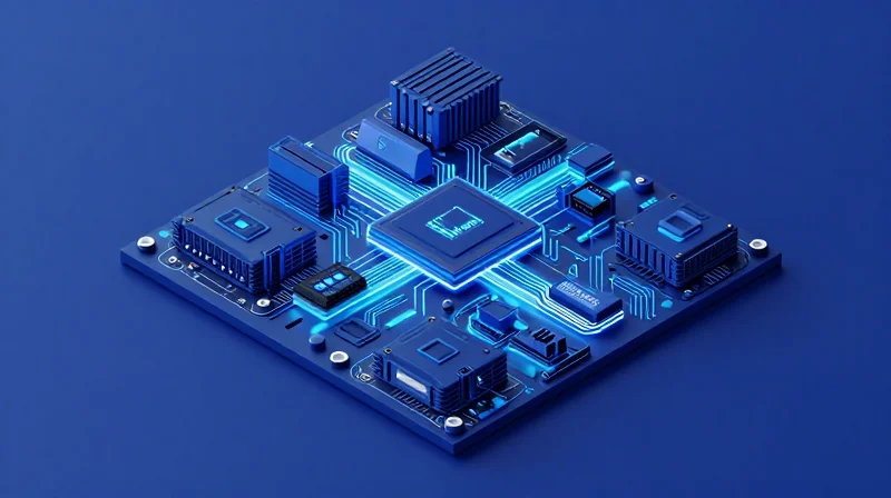
NVIDIA H100 Interconnect represents a sophisticated hierarchy of communication protocols and physical interfaces designed to synchronize thousands of Hopper-based Tensor Core GPUs into a single unified computing fabric. At its core, it leverages fourth-generation NVLink for local GPU-to-GPU data transfers, third-generation NVSwitch for multi-GPU scaling, and PCIe Gen5 for host-to-device interaction, ensuring that the H100's immense compute power is never throttled by data movement bottlenecks.
The Four Pillars of H100 Connectivity
Understanding H100 connectivity requires looking at four distinct but interconnected technologies. These components work in unison to provide the bisectional bandwidth necessary for Large Language Model (LLM) training and complex scientific simulations.
| Component | Protocol | Peak Bandwidth (Bi-dir) | Primary Purpose |
|---|---|---|---|
| NVLink 4 | NVIDIA Proprietary | 900 GB/s | GPU-to-GPU synchronization |
| NVSwitch 3 | NVIDIA Switching Fabric | 7.2 TB/s (Aggregate) | Multi-node scaling |
| PCIe Gen5 | PCI-SIG Standard | 128 GB/s | Host CPU-to-GPU data movement |
| ConnectX-7 | InfiniBand/Ethernet | 400 Gbps | External network scaling |
Intra-Node vs. Inter-Node Communication
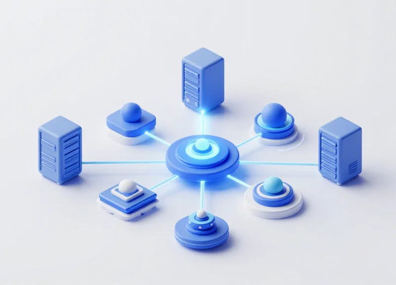
Intra-node communication is handled primarily by the NVLink fabric. In a standard DGX H100 configuration, eight GPUs are interconnected via NVSwitches, allowing any GPU to communicate with any other GPU at the full 900 GB/s rate. This effectively treats the entire 8-GPU cluster as a single compute unit with a massive shared memory pool. This is critical for model parallelism, where large neural networks are split across multiple physical chips.
For inter-node communication (connecting multiple DGX units), the H100 utilizes NVIDIA Quantum-2 InfiniBand networking. This layer relies on the ConnectX-7 SmartNIC, which offloads networking tasks from the GPU, enabling RDMA (Remote Direct Memory Access) and SHARPv3 (Scalable Hierarchical Aggregation and Reduction Protocol) to optimize collective operations like All-Reduce without taxing the GPU's compute cores.
Key Connectivity FAQs
- Is the H100 backwards compatible with older NVLink versions?
No, H100 utilizes fourth-generation NVLink, which requires specific hardware bridges and NVSwitch components designed for the Hopper architecture to achieve its peak 900 GB/s bandwidth. - How does PCIe Gen5 benefit the H100 over Gen4?
PCIe Gen5 doubles the bandwidth of its predecessor, providing 128 GB/s in a x16 slot, which significantly reduces the latency for data transfers between the system RAM and GPU memory during data ingestion. - What is the role of the NVLink Bridge?
In smaller configurations or workstations, the NVLink bridge provides a direct, high-speed point-to-point connection between two GPUs without requiring a complex external NVSwitch fabric.
NVLink 4.0: Redefining Intra-Node Bandwidth

NVLink 4.0: Redefining Intra-Node Bandwidth
NVLink 4.0 is the fourth generation of NVIDIA's proprietary high-speed interconnect technology, specifically designed to facilitate seamless peer-to-peer communication between H100 GPUs within a single server node. By providing an aggregate bandwidth of 900 GB/s—a 50% increase over the previous generation—NVLink 4.0 enables the H100 to function as part of a unified, high-performance computing cluster, effectively allowing multiple GPUs to act as a single, massive accelerator for Large Language Model (LLM) training and complex scientific simulations.
Technological Advancements in the Fourth Generation
The leap to 900 GB/s is achieved through the implementation of 18 NVLink lanes per H100 GPU, compared to 12 lanes in the previous A100 (Ampere) generation. Each lane operates at 50 GB/s total bandwidth. This architecture leverages high-speed SerDes (Serializer/Deserializer) technology to maintain signal integrity at extreme frequencies. Unlike traditional PCIe Gen5, which serves as a general-purpose bus with significant overhead, NVLink is a specialized, memory-semantic protocol optimized for GPU-to-GPU data transfers, significantly reducing latency and CPU cycles during collective operations like All-Reduce and All-to-All.
| Feature | NVLink 3.0 (A100) | NVLink 4.0 (H100) |
|---|---|---|
| Total Aggregate Bandwidth | 600 GB/s | 900 GB/s |
| Lanes per GPU | 12 | 18 |
| Bandwidth per Lane | 50 GB/s | 50 GB/s |
| Architecture Base | Ampere | Hopper |
| External Scalability | Limited to Node | Up to 256 GPUs via NVLink Switch |
Integration with the NVLink Switch System
A pivotal evolution in the H100 interconnect strategy is the synergy between NVLink 4.0 and the physical NVLink Switch System. In previous generations, NVLink was primarily restricted to intra-node (server-local) communication. With the Hopper architecture, the NVLink 4.0 protocol can be extended across multiple nodes using an external switch fabric, enabling up to 256 GPUs to communicate at full NVLink speeds. This capability is essential for training models with trillions of parameters, where the synchronization of weights and gradients across a distributed cluster is often the primary performance bottleneck.
- Is NVLink 4.0 backward compatible with A100 GPUs?
No, NVLink 4.0 is exclusive to the Hopper architecture and requires the physical and electrical specifications of the H100 GPU and its corresponding HGX H100 baseboards. - How does NVLink 4.0 compare to PCIe Gen5?
While PCIe Gen5 provides roughly 128 GB/s of bidirectional bandwidth, NVLink 4.0 offers 900 GB/s, making it approximately seven times faster for GPU-to-GPU data movement. - What role does SHARP play in NVLink 4.0?
NVLink 4.0 supports NVIDIA Scalable Hierarchical Aggregation and Reduction Protocol (SHARP) v3, which offloads collective mathematical operations from the GPU to the network fabric, further increasing effective throughput.
The Role of NVSwitch in Scalable AI Clusters
Scaling Beyond a Single Node with NVSwitch
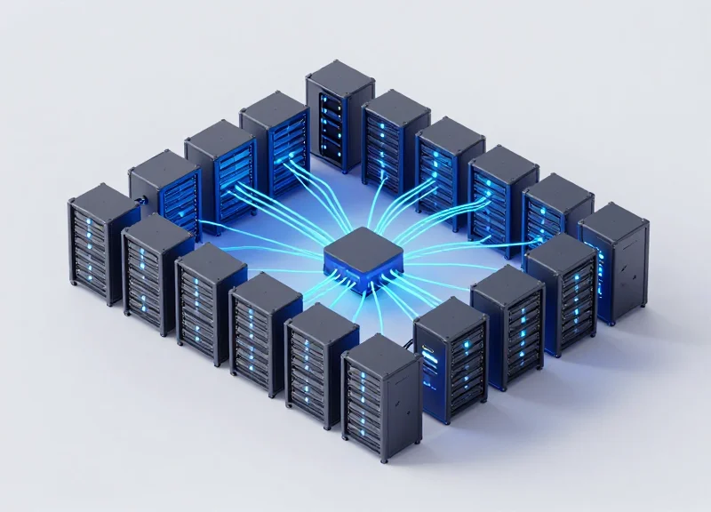
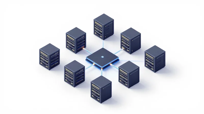
NVSwitch is the critical architectural component that extends the power of NVLink 4.0 from a simple point-to-point connection to a fully switched, non-blocking fabric. In the context of an NVIDIA H100 cluster, the 3rd-generation NVSwitch acts as a high-bandwidth crossbar that allows any GPU in the system to communicate with any other GPU at its peak native speed of 900 GB/s. This capability effectively dissolves the boundaries between individual GPU modules, allowing developers to treat a cluster of 8 or more H100 GPUs as a single, massive computational unit with a shared address space.
Technical Evolution: NVSwitch Comparison
| Specification | NVSwitch 2.0 (A100) | NVSwitch 3.0 (H100) |
|---|---|---|
| Total Aggregate Bandwidth | 4.8 TB/s | 6.4 TB/s |
| Physical NVLink Connections | 36 Ports | 64 Ports |
| SHARP Acceleration | SHARP v2 | SHARP v3 |
| In-Fabric Reduction Capacity | Limited | 2x improvement in throughput |
Hardware-Accelerated Reductions via SHARP v3
A standout feature of the H100-era NVSwitch is the Scalable Hierarchical Aggregation and Reduction Protocol (SHARP) version 3. Previously, collective operations like 'All-Reduce' required GPUs to use their own compute cycles to aggregate data. SHARP v3 offloads these mathematical operations directly into the NVSwitch silicon. By performing these reductions within the switch fabric itself, the system halves the amount of data traffic required to traverse the network and frees up H100 Tensor Cores to focus purely on training and inference tasks, significantly increasing overall cluster efficiency.
NVSwitch FAQ
- How does NVSwitch enable a seamless memory pool?
By providing a high-bandwidth, low-latency path between all GPUs, NVSwitch supports the NVLink Network protocol, which allows one GPU to directly access the HBM3 memory of another GPU without CPU intervention. - What is the maximum scalability of an H100 NVLink domain?
Using the external NVLink Switch System, NVIDIA H100 clusters can scale up to 256 GPUs in a single NVLink domain, providing 57.6 TB/s of total bisection bandwidth. - Does NVSwitch use Ethernet or InfiniBand protocols?
NVSwitch uses the proprietary NVLink protocol, which is optimized specifically for GPU-to-GPU communication, offering significantly lower overhead compared to traditional networking protocols.
InfiniBand vs. Ethernet: The Fabric Debate
The Choice of Fabric: InfiniBand vs. Ethernet
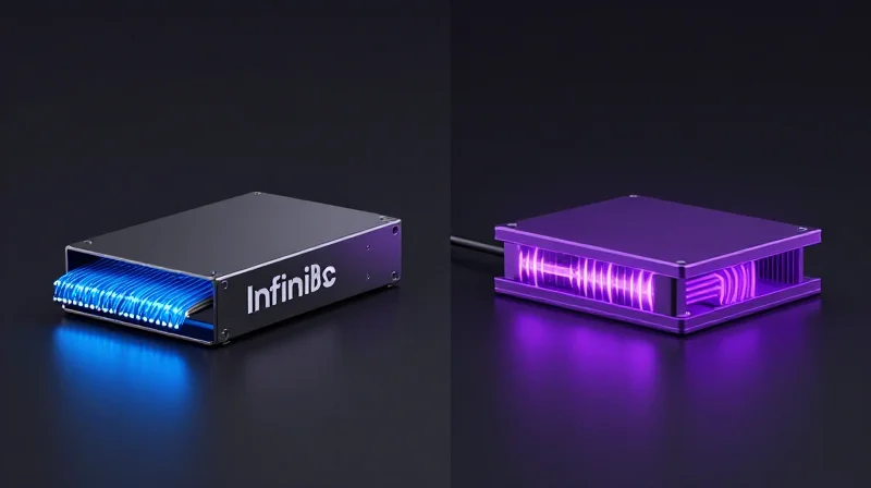
The selection between InfiniBand and Ethernet for NVIDIA H100 clusters is primarily determined by the scale of the workload and the tolerance for tail latency. InfiniBand remains the premier choice for large-scale generative AI and Large Language Model (LLM) training because of its lossless, credit-based flow control and sub-microsecond latency. Conversely, high-speed Ethernet, specifically NVIDIA Spectrum-4, has become increasingly competitive for multi-tenant cloud environments and inference workloads, leveraging RDMA over Converged Ethernet (RoCE) to narrow the performance gap with traditional HPC fabrics.
NVIDIA Quantum-2 InfiniBand: The Performance King
Quantum-2 InfiniBand is designed from the ground up for high-performance computing (HPC) and AI. It provides 400Gb/s (NDR) bandwidth and utilizes a credit-based system that prevents packet loss before it occurs. A key feature is In-Network Computing through NVIDIA SHARP (Scalable Hierarchical Aggregation and Reduction Protocol), which offloads collective operations like All-Reduce from the GPUs to the switch itself, significantly reducing the amount of data traversing the network.
NVIDIA Spectrum-4 Ethernet: The Flexible Alternative
Spectrum-4 is the industry's first 51.2 Tb/s Ethernet switch, optimized specifically for 'AI-scale' networking. While Ethernet was traditionally lossy, Spectrum-4 uses advanced features like Adaptive Routing and fine-grained Congestion Control (via Data Center Quantized Congestion Notification) to simulate the reliability of InfiniBand. This makes it ideal for enterprise data centers that require standard compatibility across diverse software stacks while still demanding the high throughput necessary for H100 GPU nodes.
| Feature | NVIDIA Quantum-2 InfiniBand | NVIDIA Spectrum-4 Ethernet |
|---|---|---|
| Primary Focus | Maximum AI Performance / Low Latency | Scalability / Interoperability |
| Flow Control | Credit-based (Lossless by design) | PFC / ECN (Lossless via RoCE) |
| Typical Latency | Sub-0.6 microseconds | 1.0 - 5.0 microseconds |
| Adaptive Routing | Hardware-native | Supported via Spectrum-4 ASIC |
| In-Network Computing | SHARP v3 Support | Limited to basic offloads |
RDMA and Congestion Management
Both fabrics rely on Remote Direct Memory Access (RDMA) to allow H100 GPUs to access memory on another node without involving the CPU, reducing overhead and latency. InfiniBand handles this natively, while Ethernet uses RoCE v2. The critical differentiator is how they handle congestion: InfiniBand avoids it through pre-allocated credits, whereas Ethernet detects and reacts to it using telemetry. For clusters exceeding 10,000 GPUs, the deterministic nature of InfiniBand often results in more predictable training times for massive models.
- When is InfiniBand necessary for H100?
InfiniBand is recommended for massive-scale training projects (e.g., GPT-4 class models) where every microsecond of communication latency impacts the total training time and cost. - Can I use standard 100G Ethernet for H100?
While technically possible, standard 100G Ethernet will severely bottleneck an H100 cluster. At least 400G networking is required to keep pace with the H100's processing power. - What is the benefit of Spectrum-4 over InfiniBand?
Spectrum-4 provides better compatibility with existing enterprise networking monitoring tools and lower TCO for providers who need to support various non-AI workloads on the same infrastructure.
Optical Transceivers and Cabling for H100
Optical Transceivers and Cabling for H100
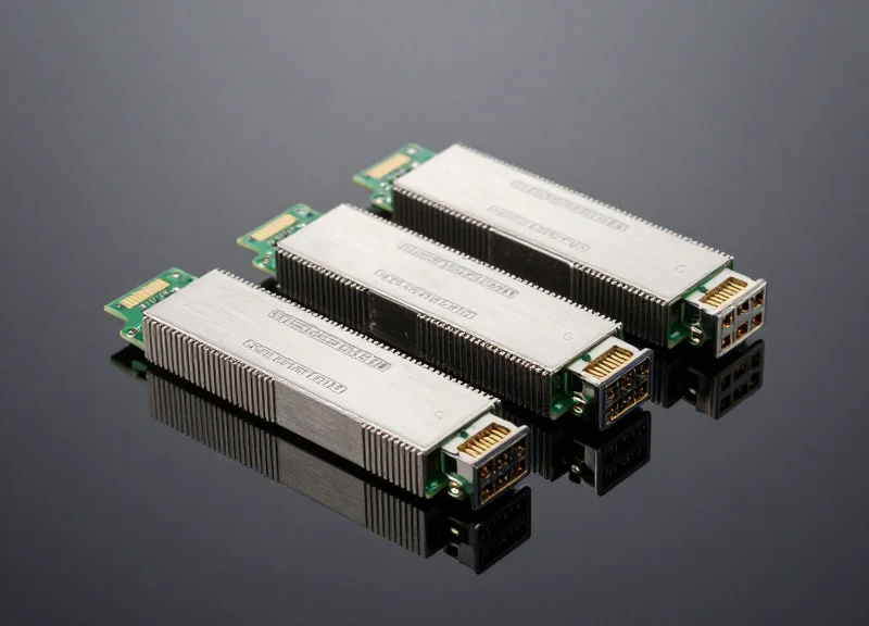
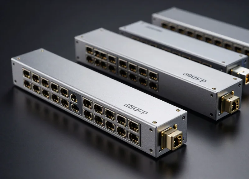
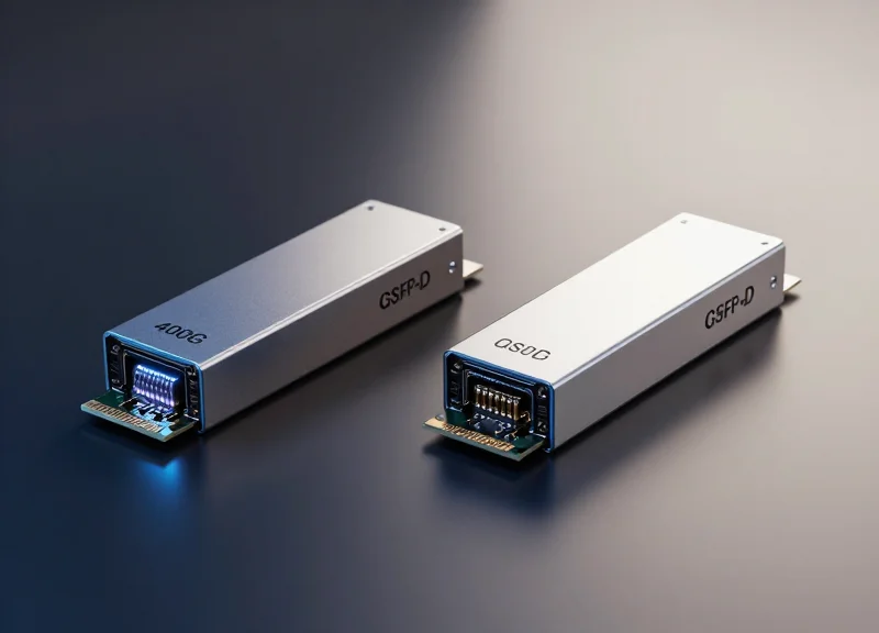
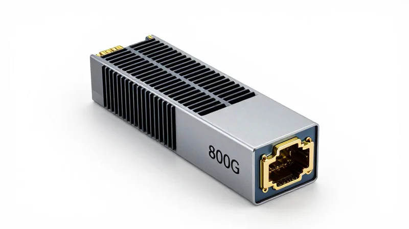
To harness the massive throughput of the NVIDIA H100, the physical layer must support 400 Gbps (NDR) and 800 Gbps speeds. This transition necessitates a move away from traditional QSFP form factors toward OSFP (Octal Small Form-factor Pluggable) to manage the significant thermal and signal integrity challenges posed by 800G optics. The H100 ecosystem utilizes a combination of Direct Attach Copper (DAC), Active Optical Cables (AOC), and discrete transceivers to maintain the low-latency requirements of the Quantum-2 InfiniBand and Spectrum-4 Ethernet platforms.
The Shift to OSFP and 800G Optics
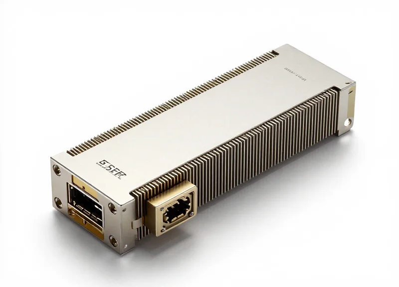
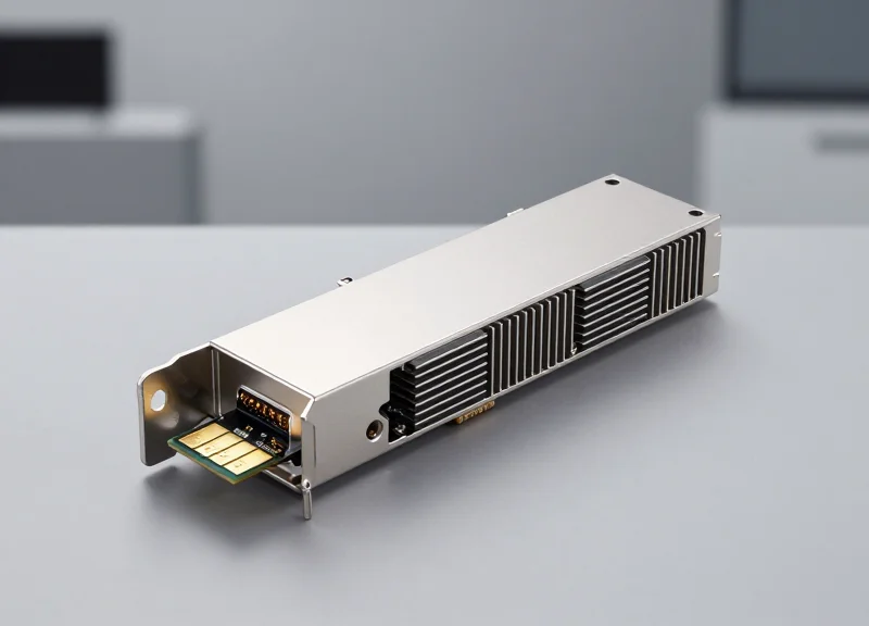
The NVIDIA H100 DGX and HGX platforms primarily utilize the OSFP form factor for 800G links. Unlike the older QSFP-DD standard, OSFP modules are slightly larger and feature an integrated heat sink. This design is crucial for AI workloads because 800G transceivers can consume up to 15-17W of power. By integrating the cooling fins directly into the module, OSFP allows for higher thermal efficiency in high-density switch environments where airflow is restricted.
| Specification | OSFP (800G) | QSFP-DD (400G) |
|---|---|---|
| Throughput | 800 Gbps per port | 400 Gbps per port |
| Thermal Dissipation | Superior (Integrated Heat Sink) | Moderate (External Cooling) |
| Lanes | 8 x 100G PAM4 | 8 x 50G or 4 x 100G |
| Primary Use Case | H100/NDR InfiniBand | A100/HDR Legacy Ethernet |
Cabling Strategies: DAC vs. AOC vs. Fiber
Selecting the right cabling depends on the physical distance between H100 nodes and switches. For connections within the same rack, Direct Attach Copper (DAC) cables are the gold standard due to their zero-power consumption and sub-nanosecond latency. For longer distances, Active Optical Cables (AOC) or discrete transceivers with fiber jumpers are required. Specifically, 800G SR8 (Short Reach) modules are used for multi-mode fiber up to 100m, while 800G DR8 (Datacenter Reach) modules utilize single-mode fiber for spans up to 500m in massive GPU clusters.
- Why is OSFP preferred over QSFP-DD for H100?
OSFP's larger surface area and integrated heat sink handle the 15W+ thermal load of 800G DSPs more effectively than QSFP-DD, which is vital for the reliability of H100 clusters. - Are H100 interconnects backward compatible?
Yes, through the use of 'Twin-port' transceivers and breakout cables (e.g., 800G to 2x400G), H100 systems can interface with older 200G (HDR) or standard 400G infrastructures. - What is the maximum distance for H100 InfiniBand cabling?
Using DAC cables, the limit is typically 2-3 meters. AOCs extend this to 30 meters, while single-mode transceivers (DR8/LR8) can reach up to 2km-10km depending on the specific optic used.
PCIe Gen5 Integration and Legacy Support
NVIDIA H100 GPUs utilize the PCIe Gen5 standard to achieve a massive 128 GB/s of throughput over a x16 link, doubling the performance of the previous PCIe 4.0 generation. This interconnect is vital for accelerating data transfers between the CPU host and GPU memory, as well as enabling high-speed access to NVMe storage via GPUDirect Storage. By adhering to the PCI Special Interest Group (PCI-SIG) standards, the H100 ensures that it can be integrated into legacy PCIe 4.0 and 3.0 systems, allowing for incremental infrastructure updates without sacrificing the ability to deploy the world's most advanced AI accelerator.
Doubling Throughput: The Shift to PCIe 5.0
As AI models grow in complexity, the demand on the system bus increases. PCIe Gen5 operates at a signaling rate of 32 GT/s per lane. For an H100 GPU using a standard x16 slot, this translates to 64 GB/s in each direction, totaling 128 GB/s of aggregate bandwidth. This bandwidth is critical for workloads involving frequent data swapping between system RAM and HBM3, such as large-scale graph analytics or recommendation systems where the dataset exceeds the GPU's local memory capacity.
| Feature | PCIe Gen 4 (A100) | PCIe Gen 5 (H100) |
|---|---|---|
| Transfer Rate | 16 GT/s | 32 GT/s |
| x16 Bandwidth (Bi-directional) | 64 GB/s | 128 GB/s |
| Encoding Efficiency | 128b/130b (~98.5%) | 128b/130b (~98.5%) |
| Typical Use Case | Standard Deep Learning | Exascale AI & LLM Training |
Architectural Flexibility and Legacy Support
A key technical advantage of the H100's PCIe implementation is its 'plug-and-play' compatibility with existing server ecosystems. The H100 PCIe card uses the standard CEM form factor, ensuring physical compatibility with previous-generation slots. At the protocol level, the PCIe controller performs an automatic negotiation (handshake) to match the highest version supported by the host motherboard.
- Backward Compatibility
The H100 can operate in PCIe 4.0 or 3.0 slots, though performance will be capped at 64 GB/s or 32 GB/s respectively. - Forward Compatibility
Designed to work seamlessly with the latest Intel Sapphire Rapids and AMD Genoa CPUs which natively support PCIe Gen5. - Signal Integrity
The H100 includes advanced equalization and re-timer support to maintain data integrity over the tighter tolerances required by 32 GT/s signals.
Frequently Asked Questions
- Will using an H100 in a PCIe 4.0 slot slow down NVLink?
No. NVLink is a separate, dedicated high-speed interconnect for GPU-to-GPU communication. Using a slower PCIe slot only affects the communication speed between the GPU and the CPU/System Storage. - Does the H100 SXM5 version also use PCIe?
Yes, while the SXM5 form factor primarily relies on NVLink for scaling, it still utilizes PCIe Gen5 lanes for command/control and data transfers from the host CPU. - Is special cabling required for PCIe Gen5?
For standard add-in cards, no special cables are needed, but the motherboard PCB must be rated for Gen5 signal speeds to avoid errors.
Practical Applications in Generative AI Training

The NVIDIA H100 interconnect architecture is the primary engine behind modern Generative AI, providing the high-bandwidth, low-latency communication required to synchronize gradients and weights across thousands of GPUs during Large Language Model (LLM) training. By utilizing fourth-generation NVLink and NDR InfiniBand, the H100 eliminates the traditional bottlenecks associated with distributed computing, effectively turning a massive data center cluster into a single, unified computational unit.
Scaling LLMs: The Transition from Single-Node to Multi-Rack
When training models with trillions of parameters, such as GPT-4 or Llama-3, no single GPU has sufficient memory or compute power. This necessitates model parallelism, where the neural network is partitioned across multiple GPUs. The H100's NVLink Switch System allows up to 256 GPUs to communicate in a single non-blocking fabric at 900 GB/s per GPU. This scale is vital for 'all-reduce' operations, where every GPU must share its calculated gradients with all other GPUs in the cluster. Without this level of interconnect performance, GPUs would spend a majority of their cycles idle, waiting for data packets to arrive over the network.
Interconnect Performance Comparison for AI Workloads
| Interconnect Type | Total Bandwidth | Primary Role in AI Training | Latency Profile |
|---|---|---|---|
| PCIe Gen5 | 128 GB/s | Host-to-GPU data transfer and local storage access | Moderate |
| NVLink 4.0 | 900 GB/s | Intra-node and Rack-scale GPU-to-GPU synchronization | Ultra-Low |
| InfiniBand NDR | 400 Gbps (per link) | Inter-node cluster networking for massive scale-out | Low/Deterministic |
The Synergy of FP8 Precision and Interconnect Throughput
The H100’s Transformer Engine introduces FP8 precision, which doubles the speed of mathematical computations compared to BF16. However, faster computation creates a 'data hunger' problem; if the interconnect cannot move data as fast as the GPU processes it, the hardware is underutilized. The H100's support for 400G NDR InfiniBand ensures that the network fabric can sustain the 2x to 4x increase in data movement demands generated by FP8 math. This synergy allows for a significant reduction in total training time (TTO), enabling researchers to iterate on model architectures in days rather than months.
FAQ: H100 Interconnect in Generative AI Training
- How does NVLink specifically speed up LLM training?
NVLink reduces the time spent on 'all-reduce' and 'all-to-all' communication primitives. By providing 7x more bandwidth than PCIe Gen5, it minimizes the communication overhead that typically plagues distributed training. - Can H100 clusters function efficiently without InfiniBand?
While smaller clusters can use Ethernet (especially Spectrum-4), InfiniBand is preferred for large-scale Generative AI because its RDMA (Remote Direct Memory Access) and adaptive routing capabilities provide the lowest possible tail latency, which is critical for synchronous training. - What is the impact of the NVLink Switch System on GPU utilization?
It allows for 'GPU-to-GPU' memory access across an entire rack, which means the collective H100 memory pool acts as a single, massive L3 cache, significantly improving the utilization of the Hopper architecture's Tensor Cores.
Future Outlook: Moving Toward Blackwell and Beyond
Future Outlook: Moving Toward Blackwell and Beyond
The NVIDIA H100 interconnect ecosystem established the standard for modern AI clusters, but the trajectory of accelerated computing is moving toward a total 'data center as a unit' philosophy. The upcoming Blackwell architecture builds directly upon the H100’s foundations, doubling the interconnect bandwidth through fifth-generation NVLink to 1.8TB/s. This evolution signifies a shift where the bottleneck is no longer the individual GPU's compute power, but the efficiency and throughput of the fabric connecting tens of thousands of processors in a unified, low-latency environment.
From Hopper to Blackwell: Interconnect Evolution
As Large Language Models (LLMs) scale toward tens of trillions of parameters, the 900GB/s limit of the H100's NVLink 4.0 becomes a critical constraint for synchronization. The move to Blackwell and beyond involves not just raw speed increases, but architectural shifts like the NVLink Switch System, which allows for significantly larger non-blocking GPU domains. This ensures that the massive data sets required for mixture-of-experts (MoE) models can move across the fabric without the overhead typically associated with traditional PCIe or Ethernet layers.
| Feature | H100 (Hopper) | B200 (Blackwell) |
|---|---|---|
| NVLink Version | 4.0 | 5.0 |
| GPU-to-GPU Bandwidth | 900 GB/s | 1.8 TB/s |
| Total Link Pairs | 18 Links | 18 Links (higher per-link speed) |
| External Network Speed | 400 Gb/s (InfiniBand/Ethernet) | 800 Gb/s (X800 Platforms) |
| Max NVLink Domain | 256 GPUs | 576 GPUs |
The Rise of 800G Networking and Silicon Photonics
The H100’s reliance on 400G networking is currently being superseded by the 800G era. NVIDIA's Quantum-X800 InfiniBand and Spectrum-X800 Ethernet platforms are designed to pair with the next generation of GPUs to maintain a 1:1 ratio between compute capacity and networking throughput. Looking further ahead, we expect a transition toward silicon photonics and co-packaged optics (CPO). This will allow interconnects to move data via light directly from the GPU package, drastically reducing power consumption and heat—the two primary enemies of H100-scale deployments.
Future Interconnect FAQ
- Will H100 interconnects be compatible with Blackwell?
While the physical infrastructure like InfiniBand switches can often support multiple generations, the fifth-generation NVLink in Blackwell is not backward compatible with the H100’s NVLink 4.0 on the same bus. - How does the interconnect impact energy efficiency?
As speeds increase, the energy cost per bit becomes vital. Future architectures aim to reduce the picojoules per bit (pJ/bit) transferred to ensure that the interconnect doesn't consume a disproportionate share of the data center's power budget. - What is the role of Liquid Cooling in future interconnects?
Higher bandwidth leads to higher heat density. Systems like the GB200 NVL72 use liquid cooling to manage the thermal output of both the GPUs and the high-speed NVLink switches integrated into the rack.
Navigating the complexities of H100 interconnects is essential for any enterprise serious about high-performance computing. By optimizing your network fabric and leveraging the latest NVLink capabilities, you can eliminate latency bottlenecks and accelerate your AI ROI. Ready to architect your next-gen data center? Contact our technical specialists for a custom optical networking consultation.